What Is Cuda Core ( Nvidia )


CUDA (or Compute Unified Device Architecture) is a parallel computing platform and application programming interface (API) that allows software to use certain types of graphics processing units (GPUs) for general purpose processing, an approach called general-purpose computing on GPUs (GPGPU). CUDA is a software layer that gives direct access to the GPU's virtual instruction set and parallel computational elements, for the execution of compute kernels.


CUDA is designed to work with programming languages such as C, C++, and Fortran. This accessibility makes it easier for specialists in parallel programming to use GPU resources, in contrast to prior APIs like Direct3D and OpenGL, which required advanced skills in graphics programming. CUDA-powered GPUs also support programming frameworks such as OpenMP, OpenACC and OpenCL; and HIP by compiling such code to CUDA.


CUDA was created by Nvidia. When it was first introduced, the name was an acronym for Compute Unified Device Architecture, but Nvidia later dropped the common use of the acronym.


What Is CUDA Cores


CUDA, which stands for Compute Unified Device Architecture, Cores are the Nvidia GPU equivalent of CPU cores that have been designed to take on multiple calculations at the same time, which is significant when you’re playing a graphically demanding game.

One CUDA Core is very similar to a CPU Core. Generally, CUDA Cores are not as developed, though they are implemented in much greater numbers, with your standard gaming CPU coming with up to 16 cores, while CUDA Cores can easily get into the hundreds.

High-end CUDA Cores can come in the thousands, with the purpose of efficient and speedy parallel computing since more CUDA Cores mean more data can be processed in parallel.

CUDA Cores can also only be found on Nvidia GPUs from the G8X series onwards, including the GeForce, Quadro and Telsa lines. It will work with most operating systems.

Cuda Programming 


Example of CUDA processing flow
Copy data from main memory to GPU memory
CPU initiates the GPU compute kernel
GPU's CUDA cores execute the kernel in parallel
Copy the resulting data from GPU memory to main memory
The CUDA platform is accessible to software developers through CUDA-accelerated libraries, compiler directives such as OpenACC, and extensions to industry-standard programming languages including C, C++ and Fortran. C/C++ programmers can use 'CUDA C/C++', compiled to PTX with nvcc, Nvidia's LLVM-based C/C++ compiler, or by clang itself.[6] Fortran programmers can use 'CUDA Fortran', compiled with the PGI CUDA Fortran compiler from The Portland Group.

In addition to libraries, compiler directives, CUDA C/C++ and CUDA Fortran, the CUDA platform supports other computational interfaces, including the Khronos Group's OpenCL,[7] Microsoft's DirectCompute, OpenGL Compute Shader and C++ AMP.[8] Third party wrappers are also available for Python, Perl, Fortran, Java, Ruby, Lua, Common Lisp, Haskell, R, MATLAB, IDL, Julia, and native support in Mathematica.

In the computer game industry, GPUs are used for graphics rendering, and for game physics calculations (physical effects such as debris, smoke, fire, fluids); examples include PhysX and Bullet. CUDA has also been used to accelerate non-graphical applications in computational biology, cryptography and other fields by an order of magnitude or more.[9][10][11][12][13]

CUDA provides both a low level API (CUDA Driver API, non single-source) and a higher level API (CUDA Runtime API, single-source). The initial CUDA SDK was made public on 15 February 2007, for Microsoft Windows and Linux. Mac OS X support was later added in version 2.0,[14] which supersedes the beta released February 14, 2008.[15] CUDA works with all Nvidia GPUs from the G8x series onwards, including GeForce, Quadro and the Tesla line. CUDA is compatible with most standard operating systems.


CUDA Cores and Stream Processors


What Nvidia calls “CUDA” encompasses more than just the physical cores on a GPU. CUDA also includes a programming language made specifically for Nvidia graphics cards so that developers can more efficiently maximize usage of Nvidia GPUs. CUDA is responsible everything you see in-game—from computing lighting and shading, to rendering your character’s model.


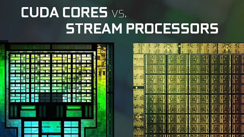
A GeForce video card, depending on family or generation, can have anywhere from several hundred to several thousand CUDA cores. The same goes for AMD and their Stream Processors. These functionally perform the same task and can be used as a metric of performance. Ultimately, both CUDA cores and Streaming Processors operate in a strictly computational capacity while a CPU core not only calculates, but also fetches from memory and decodes


Both CUDA Cores and Stream Processors are good metrics to look at when comparing inside the same family. For instance, the Radeon RX 6800 and 6900 XT have 3840 and 5120 Stream Processors respectively. And since they both belong to the same GPU architecture family, the number of Streaming Processors directly ties to performance.


Intel Tiger Lake Architecture


Tiger Lake is Intel's codename for the 11th generation Intel Core mobile processors based on the new Willow Cove Core microarchitecture, manufactured using Intel's third-generation 10 nm process node known as 10SF ("10 nm SuperFin"). Tiger Lake replaces the Ice Lake family of mobile processors, representing an Optimization step in Intel's process–architecture–optimization model.


Tiger Lake processors launched on September 2, 2020, are part of the Tiger Lake-U family and include dual-core and quad-core 9 W (7–15 W) TDP and 15 W (12–28 W) TDP models. They power 2020 "Project Athena" laptops. The quad-core 96 EU die measures 13.6 × 10.7 mm (146.1 mm2), which is 19.2% wider than the 11.4 × 10.7 mm (122.5 mm2) quad-core 64 EU Ice Lake die. The 8-core 32 EU die used in Tiger Lake-H is around 190 mm2.[8] According to Yehuda Nissan and his team, the architecture is named after a lake across Puget Sound, Washington.[9] Laptops based on Tiger Lake started to sell in October 2020.


The Tiger Lake-H35 processors were launched on January 11, 2021. These quad-core processors are designed for "ultraportable gaming" laptops with 28-35 W TDP. Intel also announced that the Tiger Lake-H processors with 45 W TDP and up to eight cores will become available in Q1 2021. Intel officially launched 11th Gen Intel Core-H series on May 11, 2021[13] and announced 11th Gen Intel Core Tiger Lake Refresh series on May 30, 2021.


Tiger Lake Processors Line-up's 


Features


CPU

Further information: Willow Cove (microarchitecture)

Intel Willow Cove CPU cores

Full memory (RAM) encryption

Indirect branch tracking and CET shadow stack

Intel Key Locker


GPU

Intel Xe-LP ("Gen12") GPU with up to 96 execution units (50% uplift compared to Ice Lake, up from 64) with some yet to be announced processors using Intel's discrete GPU, DG1

Fixed-function hardware decoding for HEVC 12-bit, 4:2:2/4:4:4; VP9 12-bit 4:4:4 and AV1 8K 10-bit 4:2:0

Support for a single 8K 12-bit HDR display or two 4K 10-bit HDR displays

Hardware accelerated Dolby Vision

Sampler Feedback support

Dual Queue Support


IPU

Image Processing Unit, a special co-processor to improve image and video capture quality

Not available on embedded models

Initially there were 1165G7, 1135G7, 1125G4 and 1115G4 models with no IPU but later embedded processors were introduced instead


I/O

PCI Express 4.0 (Pentium and Celeron CPUs are limited to PCI Express 3.0)

Integrated Thunderbolt 4 (includes USB4)

LPDDR4X-4267 memory support

LPDDR5-5400 "architecture capability" (Intel expected Tiger Lake products with LPDDR5 to be available around Q1 2021 but never released them)

Miniaturization of CPU and motherboard into an M.2 SSD-sized small circuit board


Intel Iris Xe Graphics G7 96EUs


Intel Iris Xe G7 96EUs

The Intel Xe Graphics G7 (Tiger-Lake U GPU with 96 EUs) is a integrated graphics card in the high end Tiger-Lake U CPUs (15 - 28 Watt). It is using the new Xe architecture (Gen12) and was introduced in September 2020. The GPU clocks with a base clock speed (guaranteed) of 400 MHz in all CPUs and can boost up to 1340 MHz (i7-1185G7). The slowest variant offers only 1100 MHz boost (i5-1130G7, 12 Watt TDP).


The performance depends on the TDP settings of the laptop and the used cooling. First informations show that the chip can be configured at 12 and 28 Watt TDP default (as the Ice Lake-U chips) and the performance should be around a dedicated GeForce MX350 in 3DMark benchmarks. For gaming we are expecting a bit worse performance due to the missing dedicated graphics memory and driver support. Many games e.g. had problems when testing the various laptops (e.g. Horizon Zero Dawn or Cyberpunk 2077 did not start or were crashing - see list below). Less demanding games like the Mass Effect Legendary Edition ran in medium settings fine. Compared to the older Ice Lake Iris Plus G7 GPU, the new Tiger Lake GPU should be approximately twice as fast. Therefore, the iGPU is still only for lowest graphical settings and low resolutions in demanding games.


The Tiger Lake SoCs and therefore the integrated GPU are manufactured in the modern 10nm+ (10nm SuperFin) process (improved 10nm process) at Intel and therefore should offer a very good efficiency.

Chipset ( motherboard )


In a computer system, a chipset is a set of electronic components in one or more integrated circuits known as a "Data Flow Management System"[citation needed] that manages the data flow between the processor, memory and peripherals. It is usually found on the motherboard. Chipsets are usually designed to work with a specific family of microprocessors. Because it controls communications between the processor and external devices, the chipset plays a crucial role in determining system performance.

The chipset is a silicon backbone integrated into the motherboard that works with specific CPU generations. It relays communications between the CPU and the many connected storage and expansion devices.


Details 


Living on the motherboard(opens in new tab), a PC's chipset controls the communication between the CPU, RAM(opens in new tab), storage and other peripherals. The chipset determines how many high-speed components or USB devices your best motherboard can support. Chipsets are usually comprised of one to four chips and feature controllers for commonly used peripherals, like the your keyboard(opens in new tab), mouse(opens in new tab) or monitor(opens in new tab).

PC chipsets are designed by Intel and AMD but are found on motherboards from a variety of third-party vendors, such as MSI, Asus and ASRock. Different chipsets support different CPUs, so when you're buying a CPU(opens in new tab), you have to consider that your processor will only work with motherboards using a specific chipset (and CPU socket(opens in new tab)). 

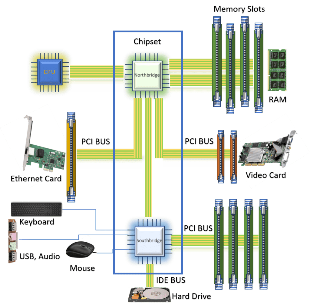
Traditionally in x86 computers, the processor's primary connection to the rest of the machine was through the motherboard chipset's northbridge. The northbridge was directly responsible for communications with high-speed devices (system memory and primary expansion buses, such as PCIe, AGP, and PCI cards, being common examples) and conversely any system communication back to the processor. This connection between the processor and northbridge is commonly designated the front-side bus (FSB). Requests to resources not directly controlled by the northbridge were offloaded to the southbridge, with the northbridge being an intermediary between the processor and the southbridge. The southbridge handled "everything else", generally lower-speed peripherals and board functions (the largest being hard disk and storage connectivity) such as USB, parallel and serial communications. In 1990s and early 2000s, the interface between a northbridge and southbridge was the PCI bus.[1]

Before 2003, any interaction between a CPU and main memory or an expansion device such as a graphics card(s) — whether AGP, PCI or integrated into the motherboard — was directly controlled by the northbridge IC on behalf of the processor. This made processor performance highly dependent on the system chipset, especially the northbridge's memory performance and ability to shuttle this information back to the processor. In 2003, however, AMD's introduction of the Athlon 64-bit series of processors[2] changed this. The Athlon64 marked the introduction of an integrated memory controller being incorporated into the processor itself thus allowing the processor to directly access and handle memory, negating the need for a traditional northbridge to do so. Intel followed suit in 2008 with the release of its Core i series CPUs and the X58 platform.


Overclocking


Keep in mind that overclocking can void your manufacturer warranty, so do some research before you get started. If you decide to do it, the right (or wrong) chipset can be the difference between achieving those speeds you want and being disappointed.

Some chipsets simply won’t work, and others will only work after installing third-party firmware. Know what you’re getting into before you invest in a motherboard or CPU for the purpose of overclocking.


Chipset vs motherboard


Some people use the term “chipset” interchangeably with “motherboard,” but they’re not the same thing. The chipset is a permanent fixture of the motherboard, but it must be compatible with the components or features you want to use. Since a chipset cannot be upgraded, the motherboard’s sockets need to fit your CPU and the chipset on the motherboard must work optimally with that CPU as well.
This is why it’s common to discuss chipset in relation to the motherboard when shopping. It's actually possible for a chipset to have capabilities greater than its paired motherboard, such as additional USB ports.


Definition of a chipset


An electronic chipset manages the flow of data between components on a motherboard. It’s the traffic controller between the CPU, GPU, RAM, storage, and peripherals. Experts have referred to it as the “glue” of the motherboard. The chipset is basically the electronics on the motherboard that communicate with all the connected components.

Most importantly, the chipset determines compatibility between all of these other components. If any of the processors or memory cards don’t communicate with the chipset, they can’t send or receive information from the motherboard.
Today’s integrated chipsets live on the motherboard and allow components to communicate with each other through the motherboard from a centralized location. But in the past, there were smaller, individualized chips for each component.
You can imagine that it was quite confusing to have a chip for the CPU, a chip for RAM, and so on. As time went on, chip functionality consolidated into two main chipsets, the faster northbridge that connects directly to the CPU and memory, and the slower southbridge.
Some functions are now absorbed by the CPU completely. The remaining components, which need their own communication bridge to the motherboard, use smaller and more efficient chipsets.


chipset lanes

If you want to expand your PC to enjoy better graphics, faster connectivity, or more memory, make sure your chipset supports it. There are only so many “lanes” on a chipset, usually between 8 and 40, and these lanes are two-way, wired connections that send data back and forth between things like a graphics card and the chipset (and then on to the motherboard).

Each component may take up many lanes, and some even take up 16 lanes at once. If your chipset doesn’t have room for everything you want to connect, you can forget about the expansion. You have to make sure that both the motherboard and the chipset have the room to make your setup work.


Random Access Memory (RAM)


Random-access memory (RAM; /ræm/) is a form of computer memory that can be read and changed in any order, typically used to store working data and machine code.[1][2] A random-access memory device allows data items to be read or written in almost the same amount of time irrespective of the physical location of data inside the memory, in contrast with other direct-access data storage media (such as hard disks, CD-RWs, DVD-RWs and the older magnetic tapes and drum memory), where the time required to read and write data items varies significantly depending on their physical locations on the recording medium, due to mechanical limitations such as media rotation speeds and arm movement.


RAM contains multiplexing and demultiplexing circuitry, to connect the data lines to the addressed storage for reading or writing the entry. Usually more than one bit of storage is accessed by the same address, and RAM devices often have multiple data lines and are said to be "8-bit" or "16-bit", etc. devices.[clarification needed]


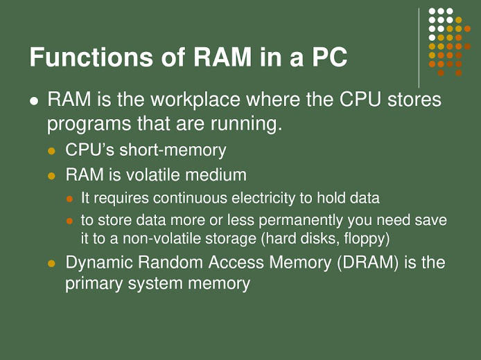
In today's technology, random-access memory takes the form of integrated circuit (IC) chips with MOS (metal-oxide-semiconductor) memory cells. RAM is normally associated with volatile types of memory (such as dynamic random-access memory (DRAM) modules), where stored information is lost if power is removed, although non-volatile RAM has also been developed. Other types of non-volatile memories exist that allow random access for read operations, but either do not allow write operations or have other kinds of limitations on them. These include most types of ROM and a type of flash memory called NOR-Flash.


The two main types of volatile random-access semiconductor memory are static random-access memory (SRAM) and dynamic random-access memory (DRAM). Commercial uses of semiconductor RAM date back to 1965, when IBM introduced the SP95 SRAM chip for their System/360 Model 95 computer, and Toshiba used DRAM memory cells for its Toscal BC-1411 electronic calculator, both based on bipolar transistors. Commercial MOS memory, based on MOS transistors, was developed in the late 1960s, and has since been the basis for all commercial semiconductor memory. The first commercial DRAM IC chip, the Intel 1103, was introduced in October 1970. Synchronous dynamic random-access memory (SDRAM) later debuted with the Samsung KM48SL2000 chip in 1992.


Highlighted 


Shadow RAM


Shadow RAM is a copy of Basic Input/Output Operating System (BIOS) routines from read-only memory (ROM) into a special area of random access memory (RAM) so that they can be accessed more quickly. Access in shadow RAM is typically in the 60-100 nanosecond range whereas ROM access is in the 125-250 ns range.

Sometimes, the contents of a relatively slow ROM chip are copied to read/write memory to allow for shorter access times. The ROM chip is then disabled while the initialized memory locations are switched in on the same block of addresses (often write-protected). This process, sometimes called shadowing, is fairly common in both computers and embedded systems.

As a common example, the BIOS in typical personal computers often has an option called “use shadow BIOS” or similar. When enabled, functions that rely on data from the BIOS's ROM instead use DRAM locations (most can also toggle shadowing of video card ROM or other ROM sections). Depending on the system, this may not result in increased performance, and may cause incompatibilities. For example, some hardware may be inaccessible to the operating system if shadow RAM is used. On some systems the benefit may be hypothetical because the BIOS is not used after booting in favor of direct hardware access. Free memory is reduced by the size of the shadowed ROMs.


Virtual memory


Most modern operating systems employ a method of extending RAM capacity, known as "virtual memory". A portion of the computer's hard drive is set aside for a paging file or a scratch partition, and the combination of physical RAM and the paging file form the system's total memory. (For example, if a computer has 2 GB (10243 B) of RAM and a 1 GB page file, the operating system has 3 GB total memory available to it.) When the system runs low on physical memory, it can "swap" portions of RAM to the paging file to make room for new data, as well as to read previously swapped information back into RAM. Excessive use of this mechanism results in thrashing and generally hampers overall system performance, mainly because hard drives are far slower than RAM.


RAM disk


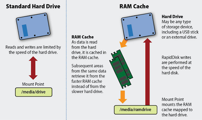
Software can "partition" a portion of a computer's RAM, allowing it to act as a much faster hard drive that is called a RAM disk. A RAM disk loses the stored data when the computer is shut down, unless memory is arranged to have a standby battery source, or changes to the RAM disk are written out to a nonvolatile disk. The RAM disk is reloaded from the physical disk upon RAM disk initialization.


DDR SDRAM


Double Data Rate Synchronous Dynamic Random-Access Memory (DDR SDRAM) is a double data rate (DDR) synchronous dynamic random-access memory (SDRAM) class of memory integrated circuits used in computers. DDR SDRAM, also retroactively called DDR1 SDRAM, has been superseded by DDR2 SDRAM, DDR3 SDRAM, DDR4 SDRAM and DDR5 SDRAM. None of its successors are forward or backward compatible with DDR1 SDRAM, meaning DDR2, DDR3, DDR4 and DDR5 memory modules will not work in DDR1-equipped motherboards, and vice versa.

Compared to single data rate (SDR) SDRAM, the DDR SDRAM interface makes higher transfer rates possible by more strict control of the timing of the electrical data and clock signals. Implementations often have to use schemes such as phase-locked loops and self-calibration to reach the required timing accuracy. The interface uses double pumping (transferring data on both the rising and falling edges of the clock signal) to double data bus bandwidth without a corresponding increase in clock frequency. One advantage of keeping the clock frequency down is that it reduces the signal integrity requirements on the circuit board connecting the memory to the controller. The name "double data rate" refers to the fact that a DDR SDRAM with a certain clock frequency achieves nearly twice the bandwidth of a SDR SDRAM running at the same clock frequency, due to this double pumping.

With data being transferred 64 bits at a time, DDR SDRAM gives a transfer rate (in bytes/s) of (memory bus clock rate) × 2 (for dual rate) × 64 (number of bits transferred) / 8 (number of bits/byte). Thus, with a bus frequency of 100 MHz, DDR SDRAM gives a maximum transfer rate of 1600 MB/s.


Dynamic Random Access Memory


Dynamic random-access memory (dynamic RAM or DRAM) is a type of random-access semiconductor memory that stores each bit of data in a memory cell, usually consisting of a tiny capacitor and a transistor, both typically based on metal-oxide-semiconductor (MOS) technology. While most DRAM memory cell designs use a capacitor and transistor, some only use two transistors. In the designs where a capacitor is used, the capacitor can either be charged or discharged; these two states are taken to represent the two values of a bit, conventionally called 0 and 1. The electric charge on the capacitors gradually leaks away; without intervention the data on the capacitor would soon be lost. To prevent this, DRAM requires an external memory refresh circuit which periodically rewrites the data in the capacitors, restoring them to their original charge. This refresh process is the defining characteristic of dynamic random-access memory, in contrast to static random-access memory (SRAM) which does not require data to be refreshed. Unlike flash memory, DRAM is volatile memory (vs. non-volatile memory), since it loses its data quickly when power is removed. However, DRAM does exhibit limited data remanence.

DRAM typically takes the form of an integrated circuit chip, which can consist of dozens to billions of DRAM memory cells. DRAM chips are widely used in digital electronics where low-cost and high-capacity computer memory is required. One of the largest applications for DRAM is the main memory (colloquially called the "RAM") in modern computers and graphics cards (where the "main memory" is called the graphics memory). It is also used in many portable devices and video game consoles. In contrast, SRAM, which is faster and more expensive than DRAM, is typically used where speed is of greater concern than cost and size, such as the cache memories in processors.


  • DRAM density

Size of the chip is measured in megabits. Most motherboards recognize only 1 GB modules if they contain 64M×8 chips (low density). If 128M×4 (high density) 1 GB modules are used, they most likely will not work. The JEDEC standard allows 128M×4 only for registered modules designed specifically for servers, but some generic manufacturers do not comply

  • Organization

PC3200 is DDR SDRAM designed to operate at 200 MHz using DDR-400 chips with a bandwidth of 3,200 MB/s. Because PC3200 memory transfers data on both the rising and falling clock edges, its effective clock rate is 400 MHz.

  • Mobile DDR

MDDR is an acronym that some enterprises use for Mobile DDR SDRAM, a type of memory used in some portable electronic devices, like mobile phones, handhelds, and digital audio players. Through techniques including reduced voltage supply and advanced refresh options, Mobile DDR can achieve greater power efficiency.


Ray Tracing ( RTX Technology ) Nvidia


In 3D computer graphics, ray tracing is a technique for modeling light transport for use in a wide variety of rendering algorithms for generating digital images.


On a spectrum of computational cost and visual fidelity, ray tracing-based rendering techniques, such as ray casting, recursive ray tracing, distribution ray tracing, photon mapping and path tracing, are generally slower and higher fidelity than scanline rendering methods. Thus, ray tracing was first deployed in applications where taking a relatively long time to render could be tolerated, such as in still computer-generated images, and film and television visual effects (VFX), but was less suited to real-time applications such as video games, where speed is critical in rendering each frame.


Since 2018, however, hardware acceleration for real-time ray tracing has become standard on new commercial graphics cards, and graphics APIs have followed suit, allowing developers to use hybrid ray tracing and rasterization-based rendering in games and other real-time applications with a lesser hit to frame render times.


Ray tracing is capable of simulating a variety of optical effects, such as reflection, refraction, soft shadows, scattering, depth of field, motion blur, caustics, ambient occlusion and dispersion phenomena (such as chromatic aberration). It can also be used to trace the path of sound waves in a similar fashion to light waves, making it a viable option for more immersive sound design in video games by rendering realistic reverberation and echoes.[4] In fact, any physical wave or particle phenomenon with approximately linear motion can be simulated with ray tracing.


Highlighted 


RTX Global Illumination


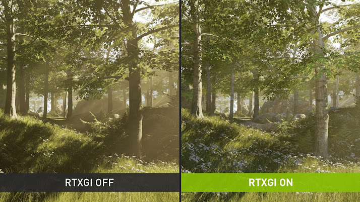
Multi-bounce indirect light without bake times, light leaks, or expensive per-frame costs. RTX Global Illumination (RTXGI) is a scalable solution that powers infinite bounce lighting in real time, even with strict frame budgets. Accelerate content creation to the speed of light with real-time in-engine lighting updates, and enjoy broad hardware support on all DirectX Raytracing (DXR)-enabled GPUs. RTXGI was built to be paired with RTX Direct Illumination (RTXDI) to create fully ray-traced scenes with an unrestrained count of dynamic light sources.


RTX Direct Illumination


Millions of dynamic lights, all fully ray traced, can be generated with RTX Direct Illumination. A real-time ray-tracing SDK, RTXDI offers photorealistic lighting of night and indoor scenes that require computing shadows from 100,000s to millions of area lights. No more baking, no more hero lights. Unlock unrestrained creativity even with limited ray-per-pixel counts. When integrated with RTXGI and NVIDIA Real-Time Denoiser (NRD), scenes benefit from breathtaking and scalable ray-traced illumination and crisp denoised images, regardless of whether the environment is indoor or outdoor, in the day or night.


Deep Learning Super Sampling


AI-powered frame rate boost delivers best-in-class image quality. NVIDIA Deep Learning Super Sampling (DLSS) leverages the power of Tensor Cores on RTX GPUs to upscale and sharpen lower-resolution input to a higher-resolution output using a generalized deep learning network trained on NVIDIA supercomputers. The result is unmatched performance and the headroom to maximize resolution and ray-tracing settings.


RT Cores And Tensor Cores


RT Cores


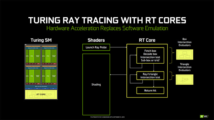
RT Cores are accelerator units that are dedicated to performing ray-tracing operations with extraordinary efficiency. Combined with NVIDIA RTX software, RT Cores enable artists to use ray-traced rendering to create photorealistic objects and environments with physically accurate lighting.


Tensor Cores


Tensor Cores enable AI on NVIDIA hardware. They’re leveraged for upscaling and sharpening with DLSS, delivering a performance boost and image quality that would be unattainable without deep learning-powered super sampling.


Ray casting algorithm


The idea behind ray casting, the predecessor to recursive ray tracing, is to trace rays from the eye, one per pixel, and find the closest object blocking the path of that ray. Think of an image as a screen-door, with each square in the screen being a pixel. This is then the object the eye sees through that pixel. Using the material properties and the effect of the lights in the scene, this algorithm can determine the shading of this object. The simplifying assumption is made that if a surface faces a light, the light will reach that surface and not be blocked or in shadow. The shading of the surface is computed using traditional 3D computer graphics shading models. One important advantage ray casting offered over older scanline algorithms was its ability to easily deal with non-planar surfaces and solids, such as cones and spheres. If a mathematical surface can be intersected by a ray, it can be rendered using ray casting. Elaborate objects can be created by using solid modeling techniques and easily rendered.

Advantages And Disadvantages


Advantages


Ray tracing-based rendering's popularity stems from its basis in a realistic simulation of light transport, as compared to other rendering methods, such as rasterization, which focuses more on the realistic simulation of geometry. Effects such as reflections and shadows, which are difficult to simulate using other algorithms, are a natural result of the ray tracing algorithm. The computational independence of each ray makes ray tracing amenable to a basic level of parallelization, but the divergence of ray paths makes high utilization under parallelism quite difficult to achieve in practice.

Disadvantages


A serious disadvantage of ray tracing is performance (though it can in theory be faster than traditional scanline rendering depending on scene complexity vs. number of pixels on-screen). Until the late 2010s, ray tracing in real time was usually considered impossible on consumer hardware for nontrivial tasks. Scanline algorithms and other algorithms use data coherence to share computations between pixels, while ray tracing normally starts the process anew, treating each eye ray separately. However, this separation offers other advantages, such as the ability to shoot more rays as needed to perform spatial anti-aliasing and improve image quality where needed.

Although it does handle interreflection and optical effects such as refraction accurately, traditional ray tracing is also not necessarily photorealistic. True photorealism occurs when the rendering equation is closely approximated or fully implemented. Implementing the rendering equation gives true photorealism, as the equation describes every physical effect of light flow. However, this is usually infeasible given the computing resources required.

The realism of all rendering methods can be evaluated as an approximation to the equation. Ray tracing, if it is limited to Whitted's algorithm, is not necessarily the most realistic. Methods that trace rays, but include additional techniques (photon mapping, path tracing), give a far more accurate simulation of real-world lighting.


Solid State Drive (SSD)


A solid-state drive (SSD) is a solid-state storage device that uses integrated circuit assemblies to store data persistently, typically using flash memory, and functioning as secondary storage in the hierarchy of computer storage. It is also sometimes called a semiconductor storage device, a solid-state device or a solid-state disk,[1] even though SSDs lack the physical spinning disks and movable read–write heads used in hard disk drives (HDDs) and floppy disks.


Compared with electromechanical drives, SSDs are typically more resistant to physical shock, run silently, and have higher input/output rates and lower latency. SSDs store data in semiconductor cells. As of 2019, cells can contain between 1 and 4 bits of data. SSD storage devices vary in their properties according to the number of bits stored in each cell, with single-bit cells ("Single Level Cells" or "SLC") being generally the most reliable, durable, fast, and expensive type, compared with 2- and 3-bit cells ("Multi-Level Cells/MLC" and "Triple-Level Cells/TLC"), and finally quad-bit cells ("QLC") being used for consumer devices that do not require such extreme properties and are the cheapest per gigabyte of the four. In addition, 3D XPoint memory (sold by Intel under the Optane brand) stores data by changing the electrical resistance of cells instead of storing electrical charges in cells, and SSDs made from RAM can be used for high speed, when data persistence after power loss is not required, or may use battery power to retain data when its usual power source is unavailable.[4] Hybrid drives or solid-state hybrid drives (SSHDs), such as Apple's Fusion Drive, combine features of SSDs and HDDs in the same unit using both flash memory and spinning magnetic disks in order to improve the performance of frequently-accessed data. Bcache achieves a similar effect purely in software, using combinations of dedicated regular SSDs and HDDs.


Highlighted:


Flash memory

Most SSD manufacturers use non-volatile NAND flash memory in the construction of their SSDs because of the lower cost compared with DRAM and the ability to retain the data without a constant power supply, ensuring data persistence through sudden power outages. Flash memory SSDs were initially slower than DRAM solutions, and some early designs were even slower than HDDs after continued use. This problem was resolved by controllers that came out in 2009 and later.


Flash-based SSDs store data in metal-oxide-semiconductor (MOS) integrated circuit chips which contain non-volatile floating-gate memory cells.[89] Flash memory-based solutions are typically packaged in standard disk drive form factors (1.8-, 2.5-, and 3.5-inch), but also in smaller more compact form factors, such as the M.2 form factor, made possible by the small size of flash memory.

Lower-priced drives usually use quad-level cell (QLC), triple-level cell (TLC) or multi-level cell (MLC) flash memory, which is slower and less reliable than single-level cell (SLC) flash memory.[90][91] This can be mitigated or even reversed by the internal design structure of the SSD, such as interleaving, changes to writing algorithms, and higher over-provisioning (more excess capacity) with which the wear-leveling algorithms can work.


DRAM

SSDs based on volatile memory such as DRAM are characterized by very fast data access, generally less than 10 microseconds, and are used primarily to accelerate applications that would otherwise be held back by the latency of flash SSDs or traditional HDDs.


DRAM-based SSDs usually incorporate either an internal battery or an external AC/DC adapter and backup storage systems to ensure data persistence while no power is being supplied to the drive from external sources. If power is lost, the battery provides power while all information is copied from random access memory (RAM) to back-up storage. When the power is restored, the information is copied back to the RAM from the back-up storage, and the SSD resumes normal operation (similar to the hibernate function used in modern operating systems).[96][97]


SSDs of this type are usually fitted with DRAM modules of the same type used in regular PCs and servers, which can be swapped out and replaced by larger modules. Such as i-RAM, HyperOs HyperDrive, DDRdrive X1, etc. Some manufacturers of DRAM SSDs solder the DRAM chips directly to the drive, and do not intend the chips to be swapped out—such as ZeusRAM, Aeon Drive, etc.


A remote, indirect memory-access disk (RIndMA Disk) uses a secondary computer with a fast network or (direct) Infiniband connection to act like a RAM-based SSD, but the new, faster, flash-memory based, SSDs already available in 2009 are making this option not as cost effective.


While the price of DRAM continues to fall, the price of Flash memory falls even faster. The "Flash becomes cheaper than DRAM" crossover point occurred approximately 2004.


3D XPoint

In 2015, Intel and Micron announced 3D XPoint as a new non-volatile memory technology. Intel released the first 3D XPoint-based drive (branded as Intel Optane SSD) in March 2017 starting with a data center product, Intel Optane SSD DC P4800X Series, and following with the client version, Intel Optane SSD 900P Series, in October 2017. Both products operate faster and with higher endurance than NAND-based SSDs, while the areal density is comparable at 128 gigabits per chip. For the price per bit, 3D XPoint is more expensive than NAND, but cheaper than DRAM.


Cache or buffer

A flash-based SSD typically uses a small amount of DRAM as a volatile cache, similar to the buffers in hard disk drives. A directory of block placement and wear leveling data is also kept in the cache while the drive is operating. One SSD controller manufacturer, SandForce, does not use an external DRAM cache on their designs but still achieves high performance. Such an elimination of the external DRAM reduces the power consumption and enables further size reduction of SSDs.


NVME SSD 

NVM Express (NVMe) or Non-Volatile Memory Host Controller Interface Specification (NVMHCIS) is an open, logical-device interface specification for accessing a computer's non-volatile storage media usually attached via PCI Express (PCIe) bus. The initialism NVM stands for non-volatile memory, which is often NAND flash memory that comes in several physical form factors, including solid-state drives (SSDs), PCI Express (PCIe) add-in cards, and M.2 cards, the successor to mSATA cards. NVM Express, as a logical-device interface, has been designed to capitalize on the low latency and internal parallelism of solid-state storage devices.


Architecturally, the logic for NVMe is physically stored within and executed by the NVMe controller chip that is physically co-located with the storage media, usually an SSD. Version changes for NVMe, e.g., 1.3 to 1.4, are incorporated within the storage media, and do not affect PCIe-compatible components such as motherboards and CPUs.


By its design, NVM Express allows host hardware and software to fully exploit the levels of parallelism possible in modern SSDs. As a result, NVM Express reduces I/O overhead and brings various performance improvements relative to previous logical-device interfaces, including multiple long command queues, and reduced latency. The previous interface protocols like AHCI were developed for use with far slower hard disk drives (HDD) where a very lengthy delay (relative to CPU operations) exists between a request and data transfer, where data speeds are much slower than RAM speeds, and where disk rotation and seek time give rise to further optimization requirements. NVM Express SSDs run hotter than 2.5" SATA SSDs and can quickly and easily reach temperatures in excess of 80 °C.


NVM Express devices are chiefly available in the form of standard-sized PCI Express expansion cards and as 2.5-inch form-factor devices that provide a four-lane PCI Express interface through the U.2 connector (formerly known as SFF-8639). Storage devices using SATA Express and the M.2 specification which support NVM Express as the logical-device interface are a popular use-case for NVMe and have become the dominant form of solid-state storage for servers, desktops, and laptops alike.


Nvidia Kepler Architecture


Kepler is the codename for a GPU microarchitecture developed by Nvidia, first introduced at retail in April 2012, as the successor to the Fermi microarchitecture. Kepler was Nvidia's first microarchitecture to focus on energy efficiency. Most GeForce 600 series, most GeForce 700 series, and some GeForce 800M series GPUs were based on Kepler, all manufactured in 28 nm. Kepler also found use in the GK20A, the GPU component of the Tegra K1 SoC, as well as in the Quadro Kxxx series, the Quadro NVS 510, and Nvidia Tesla computing modules. Kepler was followed by the Maxwell microarchitecture and used alongside Maxwell in the GeForce 700 series and GeForce 800M series.


Kepler Graphics Processors Line-up's 


Highlighted :


Next Generation Streaming Multiprocessor (SMX)


The Kepler architecture employs a new Streaming Multiprocessor Architecture called "SMX". SMXs are the reason for Kepler's power efficiency as the whole GPU uses a single unified clock speed.[5] Although SMXs usage of a single unified clock increases power efficiency due to the fact that multiple lower clock Kepler CUDA Cores consume 90% less power than multiple higher clock Fermi CUDA Core, additional processing units are needed to execute a whole warp per cycle. Doubling 16 to 32 per CUDA array solve the warp execution problem, the SMX front-end are also double with warp schedulers, dispatch unit and the register file doubled to 64K entries as to feed the additional execution units. With the risk of inflating die area, SMX PolyMorph Engines are enhanced to 2.0 rather than double alongside the execution units, enabling it to spurr polygon in shorter cycles. There are 192 shaders per SMX.[8] Dedicated FP64 CUDA cores are also used as all Kepler CUDA cores are not FP64 capable to save die space. With the improvement Nvidia made on the SMX, the results include an increase in GPU performance and efficiency. With GK110, the 48KB texture cache are unlocked for compute workloads. In compute workload the texture cache becomes a read-only data cache, specializing in unaligned memory access workloads. Furthermore, error detection capabilities have been added to make it safer for workloads that rely on ECC. The register per thread count is also doubled in GK110 with 255 registers per thread.


Microsoft Direct3D Support


Nvidia Fermi and Kepler GPUs of the GeForce 600 series support the Direct3D 11.0 specification. Nvidia originally stated that the Kepler architecture has full DirectX 11.1 support, which includes the Direct3D 11.1 path. The following "Modern UI" Direct3D 11.1 features, however, are not supported:

  • Target-Independent Rasterization (2D rendering only)
  • 16xMSAA Rasterization (2D rendering only).
  • Orthogonal Line Rendering Mode.
  • UAV (Unordered Access View) in non-pixel-shader stages.
According to the definition by Microsoft, Direct3D feature level 11_1 must be complete, otherwise the Direct3D 11.1 path can not be executed.[14] The integrated Direct3D features of the Kepler architecture are the same as those of the GeForce 400 series Fermi architecture.


Hyper-Q


Hyper-Q expands GK110 hardware work queues from 1 to 32. The significance of this being that having a single work queue meant that Fermi could be under occupied at times as there wasn't enough work in that queue to fill every SM. By having 32 work queues, GK110 can in many scenarios, achieve higher utilization by being able to put different task streams on what would otherwise be an idle SMX. The simple nature of Hyper-Q is further reinforced by the fact that it's easily mapped to MPI, a common message passing interface frequently used in HPC. As legacy MPI-based algorithms that were originally designed for multi-CPU systems that became bottlenecked by false dependencies now have a solution. By increasing the number of MPI jobs, it's possible to utilize Hyper-Q on these algorithms to improve the efficiency all without changing the code itself.


Shuffle Instructions


At a low level, GK110 sees an additional instructions and operations to further improve performance. New shuffle instructions allow for threads within a warp to share data without going back to memory, making the process much quicker than the previous load/share/store method. Atomic operations are also overhauled, speeding up the execution speed of atomic operations and adding some FP64 operations that were previously only available for FP32 data.

Dynamic Parallelism


Dynamic Parallelism ability is for kernels to be able to dispatch other kernels. With Fermi, only the CPU could dispatch a kernel, which incurs a certain amount of overhead by having to communicate back to the CPU. By giving kernels the ability to dispatch their own child kernels, GK110 can both save time by not having to go back to the CPU, and in the process free up the CPU to work on other tasks.


Video decompression/compression


NVDEC

NVENC
Main article: Nvidia NVENC
NVENC is Nvidia's power efficient fixed-function encode that is able to take codecs, decode, preprocess, and encode H.264-based content. NVENC specification input formats are limited to H.264 output. But still, NVENC, through its limited format, can support up to 4096x4096 encode.

Like Intel's Quick Sync, NVENC is currently exposed through a proprietary API, though Nvidia does have plans to provide NVENC usage through CUDA.

TXAA Support


Exclusive to Kepler GPUs, TXAA is a new anti-aliasing method from Nvidia that is designed for direct implementation into game engines. TXAA is based on the MSAA technique and custom resolve filters. It is designed to address a key problem in games known as shimmering or temporal aliasing. TXAA resolves that by smoothing out the scene in motion, making sure that any in-game scene is being cleared of any aliasing and shimmering.

GPU Boost


GPU Boost is a new feature which is roughly analogous to turbo boosting of a CPU. The GPU is always guaranteed to run at a minimum clock speed, referred to as the "base clock". This clock speed is set to the level which will ensure that the GPU stays within TDP specifications, even at maximum loads. When loads are lower, however, there is room for the clock speed to be increased without exceeding the TDP. In these scenarios, GPU Boost will gradually increase the clock speed in steps, until the GPU reaches a predefined power target (which is 170 W by default). By taking this approach, the GPU will ramp its clock up or down dynamically, so that it is providing the maximum amount of speed possible while remaining within TDP specifications.

The power target, as well as the size of the clock increase steps that the GPU will take, are both adjustable via third-party utilities and provide a means of overclocking Kepler-based cards.


NVIDIA GPUDirect


NVIDIA GPUDirect is a capability that enables GPUs within a single computer, or GPUs in different servers located across a network, to directly exchange data without needing to go to CPU/system memory. The RDMA feature in GPUDirect allows third party devices such as SSDs, NICs, and IB adapters to directly access memory on multiple GPUs within the same system, significantly decreasing the latency of MPI send and receive messages to/from GPU memory.[16] It also reduces demands on system memory bandwidth and frees the GPU DMA engines for use by other CUDA tasks. Kepler GK110 also supports other GPUDirect features including Peer‐to‐Peer and GPUDirect for Video.


Features


  • PCI Express 3.0 interface
  • DisplayPort 1.2
  • HDMI 1.4a 4K x 2K video output
  • Purevideo VP5 hardware video acceleration (up to 4K x 2K H.264 decode)
  • Hardware H.264 encoding acceleration block (NVENC)
  • Support for up to 4 independent 2D displays, or 3 stereoscopic/3D displays (NV Surround)
  • Next Generation Streaming Multiprocessor (SMX)
  • Polymorph-Engine 2.0
  • Simplified Instruction Scheduler
  • Bindless Textures
  • CUDA Compute Capability 3.0 to 3.5
  • GPU Boost (Upgraded to 2.0 on GK110)
  • TXAA Support
  • Manufactured by TSMC on a 28 nm process
  • New Shuffle Instructions
  • Dynamic Parallelism
  • Hyper-Q (Hyper-Q's MPI functionality reserve for Tesla only)
  • Grid Management Unit
  • NVIDIA GPUDirect (GPU Direct's RDMA functionality reserve for Tesla only)


Apple Iphone 14 Pro Max And A16 Bionic Specifications


The iPhone 14 Pro and iPhone 14 Pro Max are high-end smartphones designed and marketed by Apple Inc. They are the sixteenth generation flagship iPhones, succeeding the iPhone 13 Pro and iPhone 13 Pro Max. The devices were unveiled alongside the iPhone 14 and iPhone 14 Plus at the Apple Event at Apple Park in Cupertino, California on September 7, 2022 and will be made available on September 16, 2022.


The iPhone 14 Pro and iPhone 14 Pro Max are the first iPhone to have a new type of the cutout display called "Dynamic Island". iPhone 14 Pro and iPhone 14 Pro Max models (as well as the iPhone 14 and 14 Plus) sold in the United States drop support for physical SIM cards, making them the first iPhone models since the CDMA variant of the iPhone 4 to not come with a discrete SIM card reader.


Specifications 


Hardware


Chipset


The iPhone 14 Pro and Pro Max features a new A16 Bionic system on a chip (SoC), built on a 4-nanometer process, superseding the A15 Bionic seen on the iPhone 13 and 13 Pro lineup, the 3rd generation iPhone SE, and the iPhone 14 and 14 Plus.

The A16 features a 6-core CPU, made up of 2 high-performance cores and 4 high-efficiency cores. That’s the exact same count as the A15 chip.

Apple claims the A16 Bionic is the most powerful smartphone chip in the world, supposedly being 40% faster than the competition. We’re not entirely sure what Apple means by that, but this is certainly looking like a speedy chip.

Other notable upgrades include 50% more memory bandwidth, a new neural engine that can perform 17 trillion operations per second, and an Advanced ISP that will help to improve the quad‑pixel camera sensor.


GPU


A16 Bionic features an accelerated 5-core GPU with 50 percent more memory bandwidth — perfect for graphics-intensive games and apps — and a new 16-core Neural Engine capable of nearly 17 trillion operations per second.

Camera


The iPhone 14 Pro and Pro Max features a new 48-megapixel sensor, the biggest upgrade to the main camera sensor in 7 years. This allows a new 2x telephoto mode, which allows for a 2x zoom and 4k video without Digital Zoom. Apple now uses a new "Photonic Engine" for better image and video quality. The front facing camera now has autofocus, and multiple people can be recognized in a Portrait Mode shot.


Display


The iPhone model now has a Super Retina Display XDR, which peaks out at 2000 nits. The display also has a refresh rate of 120 Hz, with LTPO technology. The iPhone 14 Pro has a resolution of 2556x1179 pixels at 460 ppi, while the Pro Max variant has a 2796x1290-pixel resolution at 460 ppi. They have a fingerprint-resistant oleophobic coating with support for display of multiple languages and characters simultaneously. Both variants also support the "always on display" feature.


Battery


The iPhone 14 Pro Max provides 29 hours of video playback, while the Pro variant provides 24 hours of video playback.


Software


Like the iPhone 14 and 14 Plus, the 14 Pro and Pro Max will ship with iOS 16.


NETWORK


  • GSM / CDMA / HSPA / EVDO / LTE / 5G

LAUNCH


  • Announced 2022, September 07

Status


  • release 2022, September 16

BODY


  • Dimensions 160.7 x 77.6 x 7.9 mm (6.33 x 3.06 x 0.31 in)
  • Weight 240 g (8.47 oz)


Build

  • Glass front (Gorilla Glass), glass back (Gorilla Glass), stainless steel frame
  • SIM Dual SIM (Nano-SIM and eSIM) or Dual eSIM - International
  • Dual eSIM with multiple numbers - USA
  • Dual SIM (Nano-SIM, dual stand-by) - China
  •  IP68 dust/water resistant (up to 6m for 30 mins)
  • Apple Pay (Visa, MasterCard, AMEX certified)

DISPLAY

  • Type LTPO Super Retina XDR OLED, 120Hz, HDR10, Dolby Vision, 1000 nits (typ), 2000 nits (HBM)
  • Size 6.7 inches, 110.2 cm2 (~88.3% screen-to-body ratio)
  • Resolution 1290 x 2796 pixels, 19.5:9 ratio (~460 ppi density)
  • Protection Scratch-resistant ceramic glass, oleophobic coating

  Always-On display

PLATFORM OS iOS 16

  • Chipset Apple A16 Bionic (4 nm)
  • CPU Hexa-core (2x3.46 GHz Avalanche + 4x Blizzard)
  • GPU Apple GPU (5-core graphics)

MEMORY

  • Internal 128GB 6GB RAM, 256GB 6GB RAM, 512GB 6GB RAM, 1TB 6GB RAM

  NVMe


MAIN CAMERA

  • Quad 48 MP, f/1.8, 24mm (wide), 1.22µm, dual pixel PDAF, sensor-shift OIS
  • 12 MP, f/2.8, 77mm (telephoto), PDAF, OIS, 3x optical zoom
  • 12 MP, f/2.2, 13mm, 120˚ (ultrawide), 1.4µm, dual pixel PDAF
  • TOF 3D LiDAR scanner (depth)
  • Features Dual-LED dual-tone flash, HDR (photo/panorama)
  • Video 4K@24/25/30/60fps, 1080p@25/30/60/120/240fps, 10-bit HDR, Dolby Vision HDR (up to 60fps), ProRes, Cinematic mode (4K@30fps), stereo sound rec.

SELFIE CAMERA

  • Dual 12 MP, f/1.9, 23mm (wide), 1/3.6", PDAF
  • SL 3D, (depth/biometrics sensor)
  • Features HDR, Cinematic mode (4K@30fps)
  • Video 4K@24/25/30/60fps, 1080p@25/30/60/120fps, gyro-EIS

SOUND

  • Loudspeaker Yes, with stereo speakers
  • 3.5mm jack No

COMMS

  • WLAN Wi-Fi 802.11 a/b/g/n/ac/6, dual-band, hotspot
  • Bluetooth 5.3, A2DP, LE
  • GPS Yes, with dual-band A-GPS, GLONASS, GALILEO, BDS, QZSS
  • NFC Yes
  • Radio No
  • USB Lightning, USB 2.0

FEATURES

  • Sensors Face ID, accelerometer, gyro, proximity, compass, barometer
  •  Ultra Wideband (UWB) support
  • Emergency SOS via satellite (SMS sending/receiving)

BATTERY

  • Type Li-Ion, non-removable
  • Charging Fast charging, 50% in 30 min (advertised)
  • USB Power Delivery 2.0
  • MagSafe wireless charging 15W
  • Qi magnetic fast wireless charging 7.5W

MISC

  • Colors Space Black, Silver, Gold, Deep Purple
  • Models A2894, A2651, A2893, A2895, iphone15,3
  • Price About 1450 EUR


A16 Bionic Details 


CPU


Architecture 2x 3.2 GHz – Avalanche
4x 1.8 GHz – Blizzard
Cores 6
Frequency 3200 MHz
L1 cache 256 KB
L2 cache 32 MB
Process 4 nanometers
Transistor count 16 billion

Graphics


GPU name Apple GPU
Execution units 6

Memory


Memory type LPDDR5
Bus 4x 16 Bit
Max size 8 GB

Multimedia (ISP)


Neural processor (NPU) Neural Engine
Storage type NVMe
Max display resolution 2796 x 1290
Video capture 4K at 60FPS
Video playback 4K at 60FPS
Video codecs H.264, H.265, VP8, VP9, Motion JPEG
Audio codecs AAC, AIFF, CAF, MP3, MP4, WAV, AC-3, E-AC-3, AAX, AAX+

A neural processing unit (NPU) is a well-partitioned circuit that comprises all the control and arithmetic logic components necessary to execute machine learning algorithms. NPUs are designed to accelerate the performance of common machine learning tasks such as image classification, machine translation, object detection, and various other predictive models. NPUs may be part of a large SoC, a plurality of NPUs may be instantiated on a single chip, or they may be part of a dedicated neural-network accelerator.

Connectivity


4G support LTE Cat. 24
5G support Yes
Wi-Fi 6
Bluetooth 5.3
Navigation GPS, GLONASS, Beidou, Galileo, QZSS

Info


Announced September 2022
Class Flagship