Showing posts with label Architecture. Show all posts

Intel Tiger Lake Architecture


Tiger Lake is Intel's codename for the 11th generation Intel Core mobile processors based on the new Willow Cove Core microarchitecture, manufactured using Intel's third-generation 10 nm process node known as 10SF ("10 nm SuperFin"). Tiger Lake replaces the Ice Lake family of mobile processors, representing an Optimization step in Intel's process–architecture–optimization model.


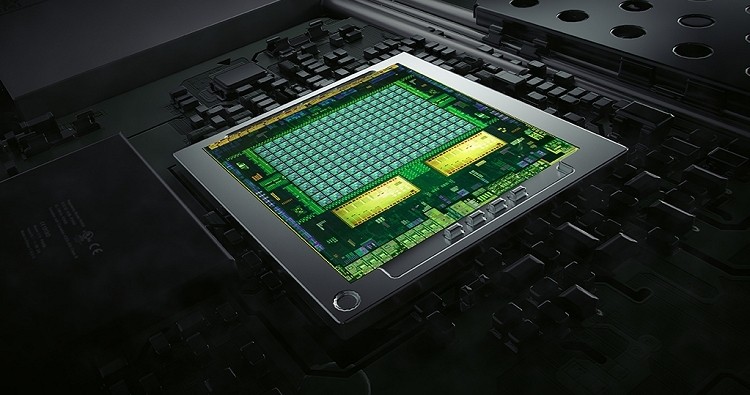
Tiger Lake processors launched on September 2, 2020, are part of the Tiger Lake-U family and include dual-core and quad-core 9 W (7–15 W) TDP and 15 W (12–28 W) TDP models. They power 2020 "Project Athena" laptops. The quad-core 96 EU die measures 13.6 × 10.7 mm (146.1 mm2), which is 19.2% wider than the 11.4 × 10.7 mm (122.5 mm2) quad-core 64 EU Ice Lake die. The 8-core 32 EU die used in Tiger Lake-H is around 190 mm2.[8] According to Yehuda Nissan and his team, the architecture is named after a lake across Puget Sound, Washington.[9] Laptops based on Tiger Lake started to sell in October 2020.


The Tiger Lake-H35 processors were launched on January 11, 2021. These quad-core processors are designed for "ultraportable gaming" laptops with 28-35 W TDP. Intel also announced that the Tiger Lake-H processors with 45 W TDP and up to eight cores will become available in Q1 2021. Intel officially launched 11th Gen Intel Core-H series on May 11, 2021[13] and announced 11th Gen Intel Core Tiger Lake Refresh series on May 30, 2021.


Tiger Lake Processors Line-up's 


Features


CPU

Further information: Willow Cove (microarchitecture)

Intel Willow Cove CPU cores

Full memory (RAM) encryption

Indirect branch tracking and CET shadow stack

Intel Key Locker


GPU

Intel Xe-LP ("Gen12") GPU with up to 96 execution units (50% uplift compared to Ice Lake, up from 64) with some yet to be announced processors using Intel's discrete GPU, DG1

Fixed-function hardware decoding for HEVC 12-bit, 4:2:2/4:4:4; VP9 12-bit 4:4:4 and AV1 8K 10-bit 4:2:0

Support for a single 8K 12-bit HDR display or two 4K 10-bit HDR displays

Hardware accelerated Dolby Vision

Sampler Feedback support

Dual Queue Support


IPU

Image Processing Unit, a special co-processor to improve image and video capture quality

Not available on embedded models

Initially there were 1165G7, 1135G7, 1125G4 and 1115G4 models with no IPU but later embedded processors were introduced instead


I/O

PCI Express 4.0 (Pentium and Celeron CPUs are limited to PCI Express 3.0)

Integrated Thunderbolt 4 (includes USB4)

LPDDR4X-4267 memory support

LPDDR5-5400 "architecture capability" (Intel expected Tiger Lake products with LPDDR5 to be available around Q1 2021 but never released them)

Miniaturization of CPU and motherboard into an M.2 SSD-sized small circuit board


Intel Iris Xe Graphics G7 96EUs


Intel Iris Xe G7 96EUs

The Intel Xe Graphics G7 (Tiger-Lake U GPU with 96 EUs) is a integrated graphics card in the high end Tiger-Lake U CPUs (15 - 28 Watt). It is using the new Xe architecture (Gen12) and was introduced in September 2020. The GPU clocks with a base clock speed (guaranteed) of 400 MHz in all CPUs and can boost up to 1340 MHz (i7-1185G7). The slowest variant offers only 1100 MHz boost (i5-1130G7, 12 Watt TDP).


The performance depends on the TDP settings of the laptop and the used cooling. First informations show that the chip can be configured at 12 and 28 Watt TDP default (as the Ice Lake-U chips) and the performance should be around a dedicated GeForce MX350 in 3DMark benchmarks. For gaming we are expecting a bit worse performance due to the missing dedicated graphics memory and driver support. Many games e.g. had problems when testing the various laptops (e.g. Horizon Zero Dawn or Cyberpunk 2077 did not start or were crashing - see list below). Less demanding games like the Mass Effect Legendary Edition ran in medium settings fine. Compared to the older Ice Lake Iris Plus G7 GPU, the new Tiger Lake GPU should be approximately twice as fast. Therefore, the iGPU is still only for lowest graphical settings and low resolutions in demanding games.


The Tiger Lake SoCs and therefore the integrated GPU are manufactured in the modern 10nm+ (10nm SuperFin) process (improved 10nm process) at Intel and therefore should offer a very good efficiency.

Nvidia Kepler Architecture


Kepler is the codename for a GPU microarchitecture developed by Nvidia, first introduced at retail in April 2012, as the successor to the Fermi microarchitecture. Kepler was Nvidia's first microarchitecture to focus on energy efficiency. Most GeForce 600 series, most GeForce 700 series, and some GeForce 800M series GPUs were based on Kepler, all manufactured in 28 nm. Kepler also found use in the GK20A, the GPU component of the Tegra K1 SoC, as well as in the Quadro Kxxx series, the Quadro NVS 510, and Nvidia Tesla computing modules. Kepler was followed by the Maxwell microarchitecture and used alongside Maxwell in the GeForce 700 series and GeForce 800M series.


Kepler Graphics Processors Line-up's 


Highlighted :


Next Generation Streaming Multiprocessor (SMX)


The Kepler architecture employs a new Streaming Multiprocessor Architecture called "SMX". SMXs are the reason for Kepler's power efficiency as the whole GPU uses a single unified clock speed.[5] Although SMXs usage of a single unified clock increases power efficiency due to the fact that multiple lower clock Kepler CUDA Cores consume 90% less power than multiple higher clock Fermi CUDA Core, additional processing units are needed to execute a whole warp per cycle. Doubling 16 to 32 per CUDA array solve the warp execution problem, the SMX front-end are also double with warp schedulers, dispatch unit and the register file doubled to 64K entries as to feed the additional execution units. With the risk of inflating die area, SMX PolyMorph Engines are enhanced to 2.0 rather than double alongside the execution units, enabling it to spurr polygon in shorter cycles. There are 192 shaders per SMX.[8] Dedicated FP64 CUDA cores are also used as all Kepler CUDA cores are not FP64 capable to save die space. With the improvement Nvidia made on the SMX, the results include an increase in GPU performance and efficiency. With GK110, the 48KB texture cache are unlocked for compute workloads. In compute workload the texture cache becomes a read-only data cache, specializing in unaligned memory access workloads. Furthermore, error detection capabilities have been added to make it safer for workloads that rely on ECC. The register per thread count is also doubled in GK110 with 255 registers per thread.


Microsoft Direct3D Support


Nvidia Fermi and Kepler GPUs of the GeForce 600 series support the Direct3D 11.0 specification. Nvidia originally stated that the Kepler architecture has full DirectX 11.1 support, which includes the Direct3D 11.1 path. The following "Modern UI" Direct3D 11.1 features, however, are not supported:

  • Target-Independent Rasterization (2D rendering only)
  • 16xMSAA Rasterization (2D rendering only).
  • Orthogonal Line Rendering Mode.
  • UAV (Unordered Access View) in non-pixel-shader stages.
According to the definition by Microsoft, Direct3D feature level 11_1 must be complete, otherwise the Direct3D 11.1 path can not be executed.[14] The integrated Direct3D features of the Kepler architecture are the same as those of the GeForce 400 series Fermi architecture.


Hyper-Q


Hyper-Q expands GK110 hardware work queues from 1 to 32. The significance of this being that having a single work queue meant that Fermi could be under occupied at times as there wasn't enough work in that queue to fill every SM. By having 32 work queues, GK110 can in many scenarios, achieve higher utilization by being able to put different task streams on what would otherwise be an idle SMX. The simple nature of Hyper-Q is further reinforced by the fact that it's easily mapped to MPI, a common message passing interface frequently used in HPC. As legacy MPI-based algorithms that were originally designed for multi-CPU systems that became bottlenecked by false dependencies now have a solution. By increasing the number of MPI jobs, it's possible to utilize Hyper-Q on these algorithms to improve the efficiency all without changing the code itself.


Shuffle Instructions


At a low level, GK110 sees an additional instructions and operations to further improve performance. New shuffle instructions allow for threads within a warp to share data without going back to memory, making the process much quicker than the previous load/share/store method. Atomic operations are also overhauled, speeding up the execution speed of atomic operations and adding some FP64 operations that were previously only available for FP32 data.

Dynamic Parallelism


Dynamic Parallelism ability is for kernels to be able to dispatch other kernels. With Fermi, only the CPU could dispatch a kernel, which incurs a certain amount of overhead by having to communicate back to the CPU. By giving kernels the ability to dispatch their own child kernels, GK110 can both save time by not having to go back to the CPU, and in the process free up the CPU to work on other tasks.


Video decompression/compression


NVDEC

NVENC
Main article: Nvidia NVENC
NVENC is Nvidia's power efficient fixed-function encode that is able to take codecs, decode, preprocess, and encode H.264-based content. NVENC specification input formats are limited to H.264 output. But still, NVENC, through its limited format, can support up to 4096x4096 encode.

Like Intel's Quick Sync, NVENC is currently exposed through a proprietary API, though Nvidia does have plans to provide NVENC usage through CUDA.

TXAA Support


Exclusive to Kepler GPUs, TXAA is a new anti-aliasing method from Nvidia that is designed for direct implementation into game engines. TXAA is based on the MSAA technique and custom resolve filters. It is designed to address a key problem in games known as shimmering or temporal aliasing. TXAA resolves that by smoothing out the scene in motion, making sure that any in-game scene is being cleared of any aliasing and shimmering.

GPU Boost


GPU Boost is a new feature which is roughly analogous to turbo boosting of a CPU. The GPU is always guaranteed to run at a minimum clock speed, referred to as the "base clock". This clock speed is set to the level which will ensure that the GPU stays within TDP specifications, even at maximum loads. When loads are lower, however, there is room for the clock speed to be increased without exceeding the TDP. In these scenarios, GPU Boost will gradually increase the clock speed in steps, until the GPU reaches a predefined power target (which is 170 W by default). By taking this approach, the GPU will ramp its clock up or down dynamically, so that it is providing the maximum amount of speed possible while remaining within TDP specifications.

The power target, as well as the size of the clock increase steps that the GPU will take, are both adjustable via third-party utilities and provide a means of overclocking Kepler-based cards.


NVIDIA GPUDirect


NVIDIA GPUDirect is a capability that enables GPUs within a single computer, or GPUs in different servers located across a network, to directly exchange data without needing to go to CPU/system memory. The RDMA feature in GPUDirect allows third party devices such as SSDs, NICs, and IB adapters to directly access memory on multiple GPUs within the same system, significantly decreasing the latency of MPI send and receive messages to/from GPU memory.[16] It also reduces demands on system memory bandwidth and frees the GPU DMA engines for use by other CUDA tasks. Kepler GK110 also supports other GPUDirect features including Peer‐to‐Peer and GPUDirect for Video.


Features


  • PCI Express 3.0 interface
  • DisplayPort 1.2
  • HDMI 1.4a 4K x 2K video output
  • Purevideo VP5 hardware video acceleration (up to 4K x 2K H.264 decode)
  • Hardware H.264 encoding acceleration block (NVENC)
  • Support for up to 4 independent 2D displays, or 3 stereoscopic/3D displays (NV Surround)
  • Next Generation Streaming Multiprocessor (SMX)
  • Polymorph-Engine 2.0
  • Simplified Instruction Scheduler
  • Bindless Textures
  • CUDA Compute Capability 3.0 to 3.5
  • GPU Boost (Upgraded to 2.0 on GK110)
  • TXAA Support
  • Manufactured by TSMC on a 28 nm process
  • New Shuffle Instructions
  • Dynamic Parallelism
  • Hyper-Q (Hyper-Q's MPI functionality reserve for Tesla only)
  • Grid Management Unit
  • NVIDIA GPUDirect (GPU Direct's RDMA functionality reserve for Tesla only)


Intel Alder Lake-S Architecture


 12th Gen Intel® Core™ CPUs adapt to the ways you work and play. When gaming, the processor prevents background tasks from interrupting or using your high-performance cores. When working, it provides a smoother system-level experience while using demanding applications.


12Th Generation Processors Line-up's [ Intel Alder Lake-S Architecture ]


Highlighted :


12th Gen CPUs integrate two types of cores into a single die: performance-cores (P-cores) and efficient-cores (E-cores).

Performance-cores :


  • Physically larger high-performance cores designed for raw speed while maintaining efficiency.
  • Optimized for low-latency single-threaded performance and AI workloads.
  • Capable of hyper-threading, or running two software threads at once.
  • Measured at 19% better performance, on average, than 11th Gen Intel® Core™ CPUs across a wide range of workloads at ISO frequency3.


Efficient-cores :


  • Physically smaller, with multiple E-cores fitting into the physical space occupied by one P-core.
  • Optimized for multi-core performance-per-watt—delivering scalable multithread performance and efficient offload of background tasks.
  • Capable of running a single software thread.
  • Capable of 40% more performance when running at the same power as a single Skylake core4.


DDR5 Memory Details :


DDR5 is the next-generation specification for RAM and it comes with a host of improvements in speed and efficiency when compared to DDR4, the current standard.

  • Higher-bandwidth kits thanks to doubled burst length—the number of bits that can be read per cycle.
  • 12th Gen supports speeds up to 4,800MHz for DDR5 and 3,200MHz for DDR4.
  • DDR5 allows capacities of up to 128GB of RAM per module, whereas DDR4 allows only 32GB.
  • DDR5 doubles the number of memory bank groups and improves the speed at which groups can be refreshed.


PCIe 5.0 :


12th Gen Intel® Core™ CPUs are at the forefront of the industry transition to PCIe 5.0. PCIe 5.0 doubles the bandwidth of 4.0, which means your system will be ready for the next generation of SSDs and discrete GPUs.

PCIe is the high-bandwidth expansion bus used to connect graphics cards, SSDs, and other peripherals to your motherboard. Each generation of PCIe doubles in throughput, with PCIe 5.0 providing theoretical maximum data transfer speeds of 32 GT/s.

  • Full backwards compatibility with PCIe 4.0 and 3.0 devices.
  • Double the bandwidth of 4.0 and four times the bandwidth of 3.0.
  • Up to 16 CPU PCIe 5.0 lanes and up to 4 CPU PCIe 4.0 lanes.


Intel UHD Graphics 64EU :


The UHD Graphics 64EU is a mobile integrated graphics solution by Intel, launched on January 4th, 2022. Built on the 10 nm process, and based on the Alder Lake GT1 graphics processor, the device supports DirectX 12. This ensures that all modern games will run on UHD Graphics 64EU. It features 512 shading units, 32 texture mapping units, and 16 ROPs. The GPU is operating at a frequency of 300 MHz, which can be boosted up to 1400 MHz.
Its power draw is rated at 45 W maximum.


General info


Of UHD Graphics 64EU's architecture, market segment and release date.

  • Place in performance rating not rated
  • Architecture Generation 12.2 (2021−2022)
  • GPU code name Alder Lake GT1
  • Market segment Desktop
  • Release date 4 January 2022 (less than a year ago)

Technical specs


  • Pipelines / CUDA cores 512 of 18432 (AD102)
  • Boost clock speed 1400 MHz of 2903 (Radeon Pro W6600)
  • Manufacturing process technology 10 nm of 4 (H100 PCIe)
  • Thermal design power (TDP) 45 Watt of 900 (Tesla S2050)
  • Texture fill rate 44.80 of 939.8 (H100 SXM5)

Memory :


  • Memory type System Shared
  • Maximum RAM amount System Shared of 128 (Radeon Instinct MI250X)
  • Memory bus width System Shared of 8192 (Radeon Instinct MI250X)
  • Memory clock speed System Shared of 21000 (GeForce RTX 3090 Ti)

API support :


DirectX 12 (12_1)
Shader Model 6.4
OpenGL 4.6
OpenCL 3.0
Vulkan 1.3


Nvidia Ampere Architecture


Ampere is the codename for a graphics processing unit (GPU) microarchitecture developed by Nvidia as the successor to both the Volta and Turing architectures, officially announced on May 14, 2020. It is named after French mathematician and physicist André-Marie Ampère. Nvidia announced the next-generation GeForce 30 series consumer GPUs at a GeForce Special Event on September 1, 2020. Nvidia announced 80GB GPU at SC20 on November 16, 2020. Mobile RTX graphics cards and the RTX 3060 were revealed on January 12, 2021. Nvidia also announced Ampere's successor, Hopper, at GTC 2022, and "Ampere Next Next" for a 2024 release at GPU Technology Conference 2021.


Ampere Graphics Processors Line-up's 

Highlighted :


Third-Generation Tensor Cores


First introduced in the NVIDIA Volta™ architecture, NVIDIA Tensor Core technology has brought dramatic speedups to AI, bringing down training times from weeks to hours and providing massive acceleration to inference. The NVIDIA Ampere architecture builds upon these innovations by bringing new precisions—Tensor Float 32 (TF32) and floating point 64 (FP64)—to accelerate and simplify AI adoption and extend the power of Tensor Cores to HPC.

TF32 works just like FP32 while delivering speedups of up to 20X for AI without requiring any code change. Using NVIDIA Automatic Mixed Precision, researchers can gain an additional 2X performance with automatic mixed precision and FP16 by adding just a couple of lines of code. And with support for bfloat16, INT8, and INT4, Tensor Cores in NVIDIA Ampere architecture Tensor Core GPUs create an incredibly versatile accelerator for both AI training and inference. Bringing the power of Tensor Cores to HPC, A100 and A30 GPUs also enable matrix operations in full, IEEE-certified, FP64 precision.


Third-Generation NVLink


Scaling applications across multiple GPUs requires extremely fast movement of data. The third generation of NVIDIA® NVLink® in the NVIDIA Ampere architecture doubles the GPU-to-GPU direct bandwidth to 600 gigabytes per second (GB/s), almost 10X higher than PCIe Gen4. When paired with the latest generation of NVIDIA NVSwitch™, all GPUs in the server can talk to each other at full NVLink speed for incredibly fast data transfers. 

NVIDIA DGX™A100 and servers from other leading computer makers take advantage of NVLink and NVSwitch technology via NVIDIA HGX™ A100 baseboards to deliver greater scalability for HPC and AI workloads.


Second-Generation RT Cores


The NVIDIA Ampere architecture’s second-generation RT Cores in the NVIDIA A40 deliver massive speedups for workloads like photorealistic rendering of movie content, architectural design evaluations, and virtual prototyping of product designs. RT Cores also speed up the rendering of ray-traced motion blur for faster results with greater visual accuracy and can simultaneously run ray tracing with either shading or denoising capabilities.


Architectural improvements of the Ampere architecture include the following:


  • CUDA Compute Capability 8.0 for A100 and 8.6 for the GeForce 30 series
  • TSMC's 7 nm FinFET process for A100
  • Custom version of Samsung's 8 nm process (8N) for the GeForce 30 series
  • Third-generation Tensor Cores with FP16, bfloat16, TensorFloat-32 (TF32) and FP64 support and sparsity acceleration. The individual Tensor cores have with 256 FP16 FMA operations per second 4x processing power (GA100 only, 2x on GA10x) compared to previous Tensor Core generations; the Tensor Core Count is reduced to one per SM.
  • Second-generation ray tracing cores; concurrent ray tracing, shading, and compute for the GeForce 30 series
  • High Bandwidth Memory 2 (HBM2) on A100 40GB & A100 80GB
  • GDDR6X memory for GeForce RTX 3090, RTX 3080 Ti, RTX 3080, RTX 3070 Ti
  • Double FP32 cores per SM on GA10x GPUs
  • NVLink 3.0 with a 50Gbit/s per pair throughput
  • PCI Express 4.0 with SR-IOV support (SR-IOV is reserved only for A100)
  • Multi-instance GPU (MIG) virtualization and GPU partitioning feature in A100 supporting up to seven instances
  • PureVideo feature set K hardware video decoding with AV1 hardware decoding for the GeForce 30 series and feature set J for A100
  • 5 NVDEC for A100
  • Adds new hardware-based 5-core JPEG decode (NVJPG) with YUV420, YUV422, YUV444, YUV400, RGBA. Should not be confused with Nvidia NVJPEG (GPU-accelerated library for JPEG encoding/decoding)


Ampere PowerFull GPU :


Nvidia GeForce RTX 3090

The GeForce RTX 3090 Ti is anenthusiast-class graphics card by NVIDIA, launched on January 27th, 2022. Built on the 8 nm process, and based on the GA102 graphics processor, in its GA102-350-A1 variant, the card supports DirectX 12 Ultimate. This ensures that all modern games will run on GeForce RTX 3090 Ti. Additionally, the DirectX 12 Ultimate capability guarantees support for hardware-raytracing, variable-rate shading and more, in upcoming video games. The GA102 graphics processor is a large chip with a die area of 628 mm² and 28,300 million transistors. It features 10752 shading units, 336 texture mapping units, and 112 ROPs. Also included are 336 tensor cores which help improve the speed of machine learning applications. The card also has 84 raytracing acceleration cores. NVIDIA has paired 24 GB GDDR6X memory with the GeForce RTX 3090 Ti, which are connected using a 384-bit memory interface. The GPU is operating at a frequency of 1560 MHz, which can be boosted up to 1860 MHz, memory is running at 1313 MHz (21 Gbps effective).

Being a triple-slot card, the NVIDIA GeForce RTX 3090 Ti draws power from 1x 16-pin power connector, with power draw rated at 450 W maximum. Display outputs include: 1x HDMI 2.1, 3x DisplayPort 1.4a. GeForce RTX 3090 Ti is connected to the rest of the system using a PCI-Express 4.0 x16 interface. The card's dimensions are 336 mm x 140 mm x 61 mm, and it features a triple-slot cooling solution. Its price at launch was 1999 US Dollars.


Ampere Vs Turing Architecture


The fastest RTX graphics cards are now alive, from Nvidia’s factory. New Nvidia Ampere GPUs, the successor of Turing are most powerful, that’s what we expect from the new-gen. Specifically, ray tracing performance has improved so much.

The Turing architecture also introduced Ray Tracing cores used to accelerate photo realistic rendering. With Ampere NVIDIA has continued to make significant improvements


Nvidia Fermi Architecture


Fermi is the codename for a graphics processing unit (GPU) microarchitecture developed by Nvidia, first released to retail in April 2010, as the successor to the Tesla microarchitecture. It was the primary microarchitecture used in the GeForce 400 series and GeForce 500 series. It was followed by Kepler, and used alongside Kepler in the GeForce 600 series, GeForce 700 series, and GeForce 800 series, in the latter two only in mobile GPUs. In the workstation market, Fermi found use in the Quadro x000 series, Quadro NVS models, as well as in Nvidia Tesla computing modules. All desktop Fermi GPUs were manufactured in 40nm, mobile Fermi GPUs in 40nm and 28nm. Fermi is the oldest microarchitecture from NVIDIA that received support for the Microsoft's rendering API Direct3D 12 feature_level 11.


Fermi Graphics Processors Line-up's 


Highlighted :


Fermi Graphic Processing Units (GPUs) feature 3.0 billion transistors and a schematic is sketched in Fig. 1

.

  • Streaming Multiprocessor (SM): composed of 32 CUDA cores (see Streaming Multiprocessor and CUDA core sections).
  • GigaThread global scheduler: distributes thread blocks to SM thread schedulers and manages the context switches between threads during execution (see Warp Scheduling section).
  • Host interface: connects the GPU to the CPU via a PCI-Express v2 bus (peak transfer rate of 8GB/s).
  • DRAM: supported up to 6GB of GDDR5 DRAM memory thanks to the 64-bit addressing capability (see Memory Architecture section).
  • Clock frequency: 1.5 GHz (not released by NVIDIA, but estimated by Insight 64).
  • Peak performance: 1.5 TFlops.
  • Global memory clock: 2 GHz.
  • DRAM bandwidth: 192GB/s.


Fermi Chips :


  • GF 100
  • GF 104
  • GF 106
  • GF 108
  • GF 110
  • GF 114
  • GF 116
  • GF 118
  • GF 119
  • GF 117


Architecture :


With these requests in mind, the Fermi team designed a processor that greatly increases raw compute horsepower, and through architectural innovations, also offers dramatically increased programmability and compute efficiency. The key architectural highlights of Fermi are:

• Third Generation Streaming Multiprocessor (SM)   

o 32 CUDA cores per SM, 4x over GT200 

o 8x the peak double precision floating point performance over GT200 

o Dual Warp Scheduler simultaneously schedules and dispatches instructions from two independent warps 

o 64 KB of RAM with a configurable partitioning of shared memory and L1 cache 


• Second Generation Parallel Thread Execution ISA 


o Unified Address Space with Full C++ Support 

o Optimized for OpenCL and DirectCompute
 
o Full IEEE 754-2008 32-bit and 64-bit precision 

o Full 32-bit integer path with 64-bit extensions 

o Memory access instructions to support transition to 64-bit addressing 

o Improved Performance through Predication 


• Improved Memory Subsystem 


o NVIDIA Parallel DataCacheTM hierarchy with Configurable L1 and Unified L2 Caches 

o First GPU with ECC memory support 

o Greatly improved atomic memory operation performance


• NVIDIA GigaThreadTM Engine


o 10x faster application context switching 

o Concurrent kernel execution o Out of Order thread block execution 

o Dual overlapped memory transfer engines 


More Details :

Optimized for OpenCL and DirectCompute 


OpenCL and DirectCompute are closely related to the CUDA programming model, sharing the key abstractions of threads, thread blocks, grids of thread blocks, barrier synchronization, perblock shared memory, global memory, and atomic operations. Fermi, a third-generation CUDA architecture, is by nature well-optimized for these APIs. In addition, Fermi offers hardware support for OpenCL and DirectCompute surface instructions with format conversion, allowing graphics and compute programs to easily operate on the same data. The PTX 2.0 ISA also adds support for the DirectCompute instructions population count, append, and bit-reverse. 


Fermi's PowerFull GPU :


  • NVIDIA GeForce GTX 590


The GeForce GTX 590 was an enthusiast-class graphics card by NVIDIA, launched on March 24th, 2011. Built on the 40 nm process, and based on the GF110 graphics processor, in its GF110-351-A1 variant, the card supports DirectX 12. Even though it supports DirectX 12, the feature level is only 11_0, which can be problematic with newer DirectX 12 titles. The GF110 graphics processor is a large chip with a die area of 520 mm² and 3,000 million transistors. GeForce GTX 590 combines two graphics processors to increase performance. It features 512 shading units, 64 texture mapping units, and 48 ROPs, per GPU. NVIDIA has paired 3,072 MB GDDR5 memory with the GeForce GTX 590, which are connected using a 384-bit memory interface per GPU (each GPU manages 1,536 MB). The GPU is operating at a frequency of 608 MHz, memory is running at 854 MHz (3.4 Gbps effective).