Showing posts with label Nvidia. Show all posts

What Is Cuda Core ( Nvidia )


CUDA (or Compute Unified Device Architecture) is a parallel computing platform and application programming interface (API) that allows software to use certain types of graphics processing units (GPUs) for general purpose processing, an approach called general-purpose computing on GPUs (GPGPU). CUDA is a software layer that gives direct access to the GPU's virtual instruction set and parallel computational elements, for the execution of compute kernels.


CUDA is designed to work with programming languages such as C, C++, and Fortran. This accessibility makes it easier for specialists in parallel programming to use GPU resources, in contrast to prior APIs like Direct3D and OpenGL, which required advanced skills in graphics programming. CUDA-powered GPUs also support programming frameworks such as OpenMP, OpenACC and OpenCL; and HIP by compiling such code to CUDA.


CUDA was created by Nvidia. When it was first introduced, the name was an acronym for Compute Unified Device Architecture, but Nvidia later dropped the common use of the acronym.
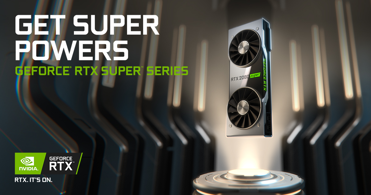


What Is CUDA Cores


CUDA, which stands for Compute Unified Device Architecture, Cores are the Nvidia GPU equivalent of CPU cores that have been designed to take on multiple calculations at the same time, which is significant when you’re playing a graphically demanding game.

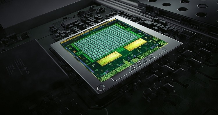
One CUDA Core is very similar to a CPU Core. Generally, CUDA Cores are not as developed, though they are implemented in much greater numbers, with your standard gaming CPU coming with up to 16 cores, while CUDA Cores can easily get into the hundreds.

High-end CUDA Cores can come in the thousands, with the purpose of efficient and speedy parallel computing since more CUDA Cores mean more data can be processed in parallel.

CUDA Cores can also only be found on Nvidia GPUs from the G8X series onwards, including the GeForce, Quadro and Telsa lines. It will work with most operating systems.

Cuda Programming 


Example of CUDA processing flow
Copy data from main memory to GPU memory
CPU initiates the GPU compute kernel
GPU's CUDA cores execute the kernel in parallel
Copy the resulting data from GPU memory to main memory
The CUDA platform is accessible to software developers through CUDA-accelerated libraries, compiler directives such as OpenACC, and extensions to industry-standard programming languages including C, C++ and Fortran. C/C++ programmers can use 'CUDA C/C++', compiled to PTX with nvcc, Nvidia's LLVM-based C/C++ compiler, or by clang itself.[6] Fortran programmers can use 'CUDA Fortran', compiled with the PGI CUDA Fortran compiler from The Portland Group.

In addition to libraries, compiler directives, CUDA C/C++ and CUDA Fortran, the CUDA platform supports other computational interfaces, including the Khronos Group's OpenCL,[7] Microsoft's DirectCompute, OpenGL Compute Shader and C++ AMP.[8] Third party wrappers are also available for Python, Perl, Fortran, Java, Ruby, Lua, Common Lisp, Haskell, R, MATLAB, IDL, Julia, and native support in Mathematica.

In the computer game industry, GPUs are used for graphics rendering, and for game physics calculations (physical effects such as debris, smoke, fire, fluids); examples include PhysX and Bullet. CUDA has also been used to accelerate non-graphical applications in computational biology, cryptography and other fields by an order of magnitude or more.[9][10][11][12][13]

CUDA provides both a low level API (CUDA Driver API, non single-source) and a higher level API (CUDA Runtime API, single-source). The initial CUDA SDK was made public on 15 February 2007, for Microsoft Windows and Linux. Mac OS X support was later added in version 2.0,[14] which supersedes the beta released February 14, 2008.[15] CUDA works with all Nvidia GPUs from the G8x series onwards, including GeForce, Quadro and the Tesla line. CUDA is compatible with most standard operating systems.


CUDA Cores and Stream Processors


What Nvidia calls “CUDA” encompasses more than just the physical cores on a GPU. CUDA also includes a programming language made specifically for Nvidia graphics cards so that developers can more efficiently maximize usage of Nvidia GPUs. CUDA is responsible everything you see in-game—from computing lighting and shading, to rendering your character’s model.


A GeForce video card, depending on family or generation, can have anywhere from several hundred to several thousand CUDA cores. The same goes for AMD and their Stream Processors. These functionally perform the same task and can be used as a metric of performance. Ultimately, both CUDA cores and Streaming Processors operate in a strictly computational capacity while a CPU core not only calculates, but also fetches from memory and decodes


Both CUDA Cores and Stream Processors are good metrics to look at when comparing inside the same family. For instance, the Radeon RX 6800 and 6900 XT have 3840 and 5120 Stream Processors respectively. And since they both belong to the same GPU architecture family, the number of Streaming Processors directly ties to performance.


Ray Tracing ( RTX Technology ) Nvidia


In 3D computer graphics, ray tracing is a technique for modeling light transport for use in a wide variety of rendering algorithms for generating digital images.


On a spectrum of computational cost and visual fidelity, ray tracing-based rendering techniques, such as ray casting, recursive ray tracing, distribution ray tracing, photon mapping and path tracing, are generally slower and higher fidelity than scanline rendering methods. Thus, ray tracing was first deployed in applications where taking a relatively long time to render could be tolerated, such as in still computer-generated images, and film and television visual effects (VFX), but was less suited to real-time applications such as video games, where speed is critical in rendering each frame.


Since 2018, however, hardware acceleration for real-time ray tracing has become standard on new commercial graphics cards, and graphics APIs have followed suit, allowing developers to use hybrid ray tracing and rasterization-based rendering in games and other real-time applications with a lesser hit to frame render times.


Ray tracing is capable of simulating a variety of optical effects, such as reflection, refraction, soft shadows, scattering, depth of field, motion blur, caustics, ambient occlusion and dispersion phenomena (such as chromatic aberration). It can also be used to trace the path of sound waves in a similar fashion to light waves, making it a viable option for more immersive sound design in video games by rendering realistic reverberation and echoes.[4] In fact, any physical wave or particle phenomenon with approximately linear motion can be simulated with ray tracing.


Highlighted 


RTX Global Illumination


Multi-bounce indirect light without bake times, light leaks, or expensive per-frame costs. RTX Global Illumination (RTXGI) is a scalable solution that powers infinite bounce lighting in real time, even with strict frame budgets. Accelerate content creation to the speed of light with real-time in-engine lighting updates, and enjoy broad hardware support on all DirectX Raytracing (DXR)-enabled GPUs. RTXGI was built to be paired with RTX Direct Illumination (RTXDI) to create fully ray-traced scenes with an unrestrained count of dynamic light sources.


RTX Direct Illumination


Millions of dynamic lights, all fully ray traced, can be generated with RTX Direct Illumination. A real-time ray-tracing SDK, RTXDI offers photorealistic lighting of night and indoor scenes that require computing shadows from 100,000s to millions of area lights. No more baking, no more hero lights. Unlock unrestrained creativity even with limited ray-per-pixel counts. When integrated with RTXGI and NVIDIA Real-Time Denoiser (NRD), scenes benefit from breathtaking and scalable ray-traced illumination and crisp denoised images, regardless of whether the environment is indoor or outdoor, in the day or night.


Deep Learning Super Sampling


AI-powered frame rate boost delivers best-in-class image quality. NVIDIA Deep Learning Super Sampling (DLSS) leverages the power of Tensor Cores on RTX GPUs to upscale and sharpen lower-resolution input to a higher-resolution output using a generalized deep learning network trained on NVIDIA supercomputers. The result is unmatched performance and the headroom to maximize resolution and ray-tracing settings.


RT Cores And Tensor Cores


RT Cores


RT Cores are accelerator units that are dedicated to performing ray-tracing operations with extraordinary efficiency. Combined with NVIDIA RTX software, RT Cores enable artists to use ray-traced rendering to create photorealistic objects and environments with physically accurate lighting.


Tensor Cores


Tensor Cores enable AI on NVIDIA hardware. They’re leveraged for upscaling and sharpening with DLSS, delivering a performance boost and image quality that would be unattainable without deep learning-powered super sampling.


Ray casting algorithm


The idea behind ray casting, the predecessor to recursive ray tracing, is to trace rays from the eye, one per pixel, and find the closest object blocking the path of that ray. Think of an image as a screen-door, with each square in the screen being a pixel. This is then the object the eye sees through that pixel. Using the material properties and the effect of the lights in the scene, this algorithm can determine the shading of this object. The simplifying assumption is made that if a surface faces a light, the light will reach that surface and not be blocked or in shadow. The shading of the surface is computed using traditional 3D computer graphics shading models. One important advantage ray casting offered over older scanline algorithms was its ability to easily deal with non-planar surfaces and solids, such as cones and spheres. If a mathematical surface can be intersected by a ray, it can be rendered using ray casting. Elaborate objects can be created by using solid modeling techniques and easily rendered.

Advantages And Disadvantages


Advantages


Ray tracing-based rendering's popularity stems from its basis in a realistic simulation of light transport, as compared to other rendering methods, such as rasterization, which focuses more on the realistic simulation of geometry. Effects such as reflections and shadows, which are difficult to simulate using other algorithms, are a natural result of the ray tracing algorithm. The computational independence of each ray makes ray tracing amenable to a basic level of parallelization, but the divergence of ray paths makes high utilization under parallelism quite difficult to achieve in practice.

Disadvantages


A serious disadvantage of ray tracing is performance (though it can in theory be faster than traditional scanline rendering depending on scene complexity vs. number of pixels on-screen). Until the late 2010s, ray tracing in real time was usually considered impossible on consumer hardware for nontrivial tasks. Scanline algorithms and other algorithms use data coherence to share computations between pixels, while ray tracing normally starts the process anew, treating each eye ray separately. However, this separation offers other advantages, such as the ability to shoot more rays as needed to perform spatial anti-aliasing and improve image quality where needed.

Although it does handle interreflection and optical effects such as refraction accurately, traditional ray tracing is also not necessarily photorealistic. True photorealism occurs when the rendering equation is closely approximated or fully implemented. Implementing the rendering equation gives true photorealism, as the equation describes every physical effect of light flow. However, this is usually infeasible given the computing resources required.

The realism of all rendering methods can be evaluated as an approximation to the equation. Ray tracing, if it is limited to Whitted's algorithm, is not necessarily the most realistic. Methods that trace rays, but include additional techniques (photon mapping, path tracing), give a far more accurate simulation of real-world lighting.


Nvidia Kepler Architecture


Kepler is the codename for a GPU microarchitecture developed by Nvidia, first introduced at retail in April 2012, as the successor to the Fermi microarchitecture. Kepler was Nvidia's first microarchitecture to focus on energy efficiency. Most GeForce 600 series, most GeForce 700 series, and some GeForce 800M series GPUs were based on Kepler, all manufactured in 28 nm. Kepler also found use in the GK20A, the GPU component of the Tegra K1 SoC, as well as in the Quadro Kxxx series, the Quadro NVS 510, and Nvidia Tesla computing modules. Kepler was followed by the Maxwell microarchitecture and used alongside Maxwell in the GeForce 700 series and GeForce 800M series.


Kepler Graphics Processors Line-up's 


Highlighted :


Next Generation Streaming Multiprocessor (SMX)


The Kepler architecture employs a new Streaming Multiprocessor Architecture called "SMX". SMXs are the reason for Kepler's power efficiency as the whole GPU uses a single unified clock speed.[5] Although SMXs usage of a single unified clock increases power efficiency due to the fact that multiple lower clock Kepler CUDA Cores consume 90% less power than multiple higher clock Fermi CUDA Core, additional processing units are needed to execute a whole warp per cycle. Doubling 16 to 32 per CUDA array solve the warp execution problem, the SMX front-end are also double with warp schedulers, dispatch unit and the register file doubled to 64K entries as to feed the additional execution units. With the risk of inflating die area, SMX PolyMorph Engines are enhanced to 2.0 rather than double alongside the execution units, enabling it to spurr polygon in shorter cycles. There are 192 shaders per SMX.[8] Dedicated FP64 CUDA cores are also used as all Kepler CUDA cores are not FP64 capable to save die space. With the improvement Nvidia made on the SMX, the results include an increase in GPU performance and efficiency. With GK110, the 48KB texture cache are unlocked for compute workloads. In compute workload the texture cache becomes a read-only data cache, specializing in unaligned memory access workloads. Furthermore, error detection capabilities have been added to make it safer for workloads that rely on ECC. The register per thread count is also doubled in GK110 with 255 registers per thread.


Microsoft Direct3D Support


Nvidia Fermi and Kepler GPUs of the GeForce 600 series support the Direct3D 11.0 specification. Nvidia originally stated that the Kepler architecture has full DirectX 11.1 support, which includes the Direct3D 11.1 path. The following "Modern UI" Direct3D 11.1 features, however, are not supported:

  • Target-Independent Rasterization (2D rendering only)
  • 16xMSAA Rasterization (2D rendering only).
  • Orthogonal Line Rendering Mode.
  • UAV (Unordered Access View) in non-pixel-shader stages.
According to the definition by Microsoft, Direct3D feature level 11_1 must be complete, otherwise the Direct3D 11.1 path can not be executed.[14] The integrated Direct3D features of the Kepler architecture are the same as those of the GeForce 400 series Fermi architecture.


Hyper-Q


Hyper-Q expands GK110 hardware work queues from 1 to 32. The significance of this being that having a single work queue meant that Fermi could be under occupied at times as there wasn't enough work in that queue to fill every SM. By having 32 work queues, GK110 can in many scenarios, achieve higher utilization by being able to put different task streams on what would otherwise be an idle SMX. The simple nature of Hyper-Q is further reinforced by the fact that it's easily mapped to MPI, a common message passing interface frequently used in HPC. As legacy MPI-based algorithms that were originally designed for multi-CPU systems that became bottlenecked by false dependencies now have a solution. By increasing the number of MPI jobs, it's possible to utilize Hyper-Q on these algorithms to improve the efficiency all without changing the code itself.


Shuffle Instructions


At a low level, GK110 sees an additional instructions and operations to further improve performance. New shuffle instructions allow for threads within a warp to share data without going back to memory, making the process much quicker than the previous load/share/store method. Atomic operations are also overhauled, speeding up the execution speed of atomic operations and adding some FP64 operations that were previously only available for FP32 data.

Dynamic Parallelism


Dynamic Parallelism ability is for kernels to be able to dispatch other kernels. With Fermi, only the CPU could dispatch a kernel, which incurs a certain amount of overhead by having to communicate back to the CPU. By giving kernels the ability to dispatch their own child kernels, GK110 can both save time by not having to go back to the CPU, and in the process free up the CPU to work on other tasks.


Video decompression/compression


NVDEC

NVENC
Main article: Nvidia NVENC
NVENC is Nvidia's power efficient fixed-function encode that is able to take codecs, decode, preprocess, and encode H.264-based content. NVENC specification input formats are limited to H.264 output. But still, NVENC, through its limited format, can support up to 4096x4096 encode.

Like Intel's Quick Sync, NVENC is currently exposed through a proprietary API, though Nvidia does have plans to provide NVENC usage through CUDA.

TXAA Support


Exclusive to Kepler GPUs, TXAA is a new anti-aliasing method from Nvidia that is designed for direct implementation into game engines. TXAA is based on the MSAA technique and custom resolve filters. It is designed to address a key problem in games known as shimmering or temporal aliasing. TXAA resolves that by smoothing out the scene in motion, making sure that any in-game scene is being cleared of any aliasing and shimmering.

GPU Boost


GPU Boost is a new feature which is roughly analogous to turbo boosting of a CPU. The GPU is always guaranteed to run at a minimum clock speed, referred to as the "base clock". This clock speed is set to the level which will ensure that the GPU stays within TDP specifications, even at maximum loads. When loads are lower, however, there is room for the clock speed to be increased without exceeding the TDP. In these scenarios, GPU Boost will gradually increase the clock speed in steps, until the GPU reaches a predefined power target (which is 170 W by default). By taking this approach, the GPU will ramp its clock up or down dynamically, so that it is providing the maximum amount of speed possible while remaining within TDP specifications.

The power target, as well as the size of the clock increase steps that the GPU will take, are both adjustable via third-party utilities and provide a means of overclocking Kepler-based cards.


NVIDIA GPUDirect


NVIDIA GPUDirect is a capability that enables GPUs within a single computer, or GPUs in different servers located across a network, to directly exchange data without needing to go to CPU/system memory. The RDMA feature in GPUDirect allows third party devices such as SSDs, NICs, and IB adapters to directly access memory on multiple GPUs within the same system, significantly decreasing the latency of MPI send and receive messages to/from GPU memory.[16] It also reduces demands on system memory bandwidth and frees the GPU DMA engines for use by other CUDA tasks. Kepler GK110 also supports other GPUDirect features including Peer‐to‐Peer and GPUDirect for Video.


Features


  • PCI Express 3.0 interface
  • DisplayPort 1.2
  • HDMI 1.4a 4K x 2K video output
  • Purevideo VP5 hardware video acceleration (up to 4K x 2K H.264 decode)
  • Hardware H.264 encoding acceleration block (NVENC)
  • Support for up to 4 independent 2D displays, or 3 stereoscopic/3D displays (NV Surround)
  • Next Generation Streaming Multiprocessor (SMX)
  • Polymorph-Engine 2.0
  • Simplified Instruction Scheduler
  • Bindless Textures
  • CUDA Compute Capability 3.0 to 3.5
  • GPU Boost (Upgraded to 2.0 on GK110)
  • TXAA Support
  • Manufactured by TSMC on a 28 nm process
  • New Shuffle Instructions
  • Dynamic Parallelism
  • Hyper-Q (Hyper-Q's MPI functionality reserve for Tesla only)
  • Grid Management Unit
  • NVIDIA GPUDirect (GPU Direct's RDMA functionality reserve for Tesla only)


Nvidia Ampere Architecture


Ampere is the codename for a graphics processing unit (GPU) microarchitecture developed by Nvidia as the successor to both the Volta and Turing architectures, officially announced on May 14, 2020. It is named after French mathematician and physicist André-Marie Ampère. Nvidia announced the next-generation GeForce 30 series consumer GPUs at a GeForce Special Event on September 1, 2020. Nvidia announced 80GB GPU at SC20 on November 16, 2020. Mobile RTX graphics cards and the RTX 3060 were revealed on January 12, 2021. Nvidia also announced Ampere's successor, Hopper, at GTC 2022, and "Ampere Next Next" for a 2024 release at GPU Technology Conference 2021.


Ampere Graphics Processors Line-up's 

Highlighted :


Third-Generation Tensor Cores


First introduced in the NVIDIA Volta™ architecture, NVIDIA Tensor Core technology has brought dramatic speedups to AI, bringing down training times from weeks to hours and providing massive acceleration to inference. The NVIDIA Ampere architecture builds upon these innovations by bringing new precisions—Tensor Float 32 (TF32) and floating point 64 (FP64)—to accelerate and simplify AI adoption and extend the power of Tensor Cores to HPC.

TF32 works just like FP32 while delivering speedups of up to 20X for AI without requiring any code change. Using NVIDIA Automatic Mixed Precision, researchers can gain an additional 2X performance with automatic mixed precision and FP16 by adding just a couple of lines of code. And with support for bfloat16, INT8, and INT4, Tensor Cores in NVIDIA Ampere architecture Tensor Core GPUs create an incredibly versatile accelerator for both AI training and inference. Bringing the power of Tensor Cores to HPC, A100 and A30 GPUs also enable matrix operations in full, IEEE-certified, FP64 precision.


Third-Generation NVLink


Scaling applications across multiple GPUs requires extremely fast movement of data. The third generation of NVIDIA® NVLink® in the NVIDIA Ampere architecture doubles the GPU-to-GPU direct bandwidth to 600 gigabytes per second (GB/s), almost 10X higher than PCIe Gen4. When paired with the latest generation of NVIDIA NVSwitch™, all GPUs in the server can talk to each other at full NVLink speed for incredibly fast data transfers. 

NVIDIA DGX™A100 and servers from other leading computer makers take advantage of NVLink and NVSwitch technology via NVIDIA HGX™ A100 baseboards to deliver greater scalability for HPC and AI workloads.


Second-Generation RT Cores


The NVIDIA Ampere architecture’s second-generation RT Cores in the NVIDIA A40 deliver massive speedups for workloads like photorealistic rendering of movie content, architectural design evaluations, and virtual prototyping of product designs. RT Cores also speed up the rendering of ray-traced motion blur for faster results with greater visual accuracy and can simultaneously run ray tracing with either shading or denoising capabilities.


Architectural improvements of the Ampere architecture include the following:


  • CUDA Compute Capability 8.0 for A100 and 8.6 for the GeForce 30 series
  • TSMC's 7 nm FinFET process for A100
  • Custom version of Samsung's 8 nm process (8N) for the GeForce 30 series
  • Third-generation Tensor Cores with FP16, bfloat16, TensorFloat-32 (TF32) and FP64 support and sparsity acceleration. The individual Tensor cores have with 256 FP16 FMA operations per second 4x processing power (GA100 only, 2x on GA10x) compared to previous Tensor Core generations; the Tensor Core Count is reduced to one per SM.
  • Second-generation ray tracing cores; concurrent ray tracing, shading, and compute for the GeForce 30 series
  • High Bandwidth Memory 2 (HBM2) on A100 40GB & A100 80GB
  • GDDR6X memory for GeForce RTX 3090, RTX 3080 Ti, RTX 3080, RTX 3070 Ti
  • Double FP32 cores per SM on GA10x GPUs
  • NVLink 3.0 with a 50Gbit/s per pair throughput
  • PCI Express 4.0 with SR-IOV support (SR-IOV is reserved only for A100)
  • Multi-instance GPU (MIG) virtualization and GPU partitioning feature in A100 supporting up to seven instances
  • PureVideo feature set K hardware video decoding with AV1 hardware decoding for the GeForce 30 series and feature set J for A100
  • 5 NVDEC for A100
  • Adds new hardware-based 5-core JPEG decode (NVJPG) with YUV420, YUV422, YUV444, YUV400, RGBA. Should not be confused with Nvidia NVJPEG (GPU-accelerated library for JPEG encoding/decoding)


Ampere PowerFull GPU :


Nvidia GeForce RTX 3090

The GeForce RTX 3090 Ti is anenthusiast-class graphics card by NVIDIA, launched on January 27th, 2022. Built on the 8 nm process, and based on the GA102 graphics processor, in its GA102-350-A1 variant, the card supports DirectX 12 Ultimate. This ensures that all modern games will run on GeForce RTX 3090 Ti. Additionally, the DirectX 12 Ultimate capability guarantees support for hardware-raytracing, variable-rate shading and more, in upcoming video games. The GA102 graphics processor is a large chip with a die area of 628 mm² and 28,300 million transistors. It features 10752 shading units, 336 texture mapping units, and 112 ROPs. Also included are 336 tensor cores which help improve the speed of machine learning applications. The card also has 84 raytracing acceleration cores. NVIDIA has paired 24 GB GDDR6X memory with the GeForce RTX 3090 Ti, which are connected using a 384-bit memory interface. The GPU is operating at a frequency of 1560 MHz, which can be boosted up to 1860 MHz, memory is running at 1313 MHz (21 Gbps effective).

Being a triple-slot card, the NVIDIA GeForce RTX 3090 Ti draws power from 1x 16-pin power connector, with power draw rated at 450 W maximum. Display outputs include: 1x HDMI 2.1, 3x DisplayPort 1.4a. GeForce RTX 3090 Ti is connected to the rest of the system using a PCI-Express 4.0 x16 interface. The card's dimensions are 336 mm x 140 mm x 61 mm, and it features a triple-slot cooling solution. Its price at launch was 1999 US Dollars.


Ampere Vs Turing Architecture


The fastest RTX graphics cards are now alive, from Nvidia’s factory. New Nvidia Ampere GPUs, the successor of Turing are most powerful, that’s what we expect from the new-gen. Specifically, ray tracing performance has improved so much.

The Turing architecture also introduced Ray Tracing cores used to accelerate photo realistic rendering. With Ampere NVIDIA has continued to make significant improvements


Nvidia Introduction

Introduction Of Nvidia :


Nvidia Corporation commonly known as Nvidia, is an American multinational technology company incorporated in Delaware and based in Santa ClaraCalifornia. It is a software and fabless company which designs graphics processing units (GPUs), application programming interface (APIs) for data science and high-performance computing as well as system on a chip units (SoCs) for the mobile computing and automotive market. Nvidia is a global leader in artificial intelligence hardware and software. Its professional line of GPUs are used in workstations for applications in such fields as architecture, engineering and construction, media and entertainment, automotive, scientific research, and manufacturing design.

In addition to GPU manufacturing, Nvidia provides an API called CUDA that allows the creation of massively parallel programs which utilize GPUs. They are deployed in supercomputing sites around the world. More recently, it has moved into the mobile computing market, where it produces Tegra mobile processors for smartphones and tablets as well as vehicle navigation and entertainment systems.In addition to AMD, its competitors include Intel, Qualcomm and AI-accelerator companies such as Graphcore.


Architectures :


Features 


Geforce Model's :


Nvidia RTX :


NVIDIA RTX technology empowers developers to redefine what's possible in computer graphics, video, and imaging. Accelerate application development by leveraging the powerful new ray tracing, deep learning, and rasterization capabilities through industry-leading software Platforms, SDKs and APIs.


Nvidia GTX :


GTX stands for Giga Texel Shader eXtreme and is a variant under the brand GeForce owned by Nvidia. They were first introduced in 2008 with series 200, codenamed Tesla. The first product in this series was GTX 260 and more expensive GTX 280. The introduction of these cards also affected the naming scheme and from the release of these cards onwards, Nvidia GPUs used a naming scheme that has GTX/GT as a prefix followed by their model number. With every other major release in the series, Nvidia changed its microarchitecture on which its cards are based on i.e. series 200 & 300 were based on Tesla architecture, series 400 & 500 were based on Fermi architecture and so on.
The latest GTX series 16, consist of GTX 1650, GTX 1660, GTX 1660Ti, and its Super counterparts. These are based on Turing architecture and were introduced in 2019.


Nvidia GTS :


Built from the ground up for next generation DX11 gaming, the GeForce GTS 450 delivers revolutionary tessellation performance for the ultimate gaming experience. With full support for NVIDIA 3D Vision the GeForce GTS 450 provides the graphics horsepower and video bandwidth needed to experience games and high definition Blu-ray movies in eye-popping stereoscopic 3D.


Nvidia GT :


The Gigabyte GeForce GT 1030 is one of the best entry-level GPUs. With its ultra-durable components, this GPU offers outstanding performance without compromising the system's lifespan. If you are a gaming enthusiast, you will love this GPU.


The First Graphics Processor Of Nvidia :


  • GeForce 256


The term GPU has been in use since at least the 1980s. Nvidia popularized it in 1999 by marketing the GeForce 256 add-in board (AIB) as the world’s first GPU. It offered integrated transform, lighting, triangle setup/clipping, and rendering engines as a single-chip processor.

Very-large-scale integrated circuitry—VLSI, started taking hold in the early 1990s. As the number of transistors engineers could incorporate on a single chip increased almost exponentially, the number of functions in the CPU and the graphics processor increased. One of the biggest consumers of the CPU was graphics transformation compute elements into graphics processors. Architects from various graphics chip companies decided transform and lighting (T&L) was a function that should be in the graphics processor. The operation was known at the time as transform and lighting (T&L). A T&L engine is a vertex shader and a geometry translator—many names for the little FFP.


Geforce 256 Specifications :


The GeForce 256 SDR was a graphics card by NVIDIA, launched on October 11th, 1999. Built on the 220 nm process, and based on the NV10 graphics processor, the card supports DirectX 7.0. Since GeForce 256 SDR does not support DirectX 11 or DirectX 12, it might not be able to run all the latest games. The NV10 graphics processor is an average sized chip with a die area of 139 mm² and 17 million transistors. It features 4 pixel shaders and 0 vertex shaders, 4 texture mapping units, and 4 ROPs. Due to the lack of unified shaders you will not be able to run recent games at all (which require unified shader/DX10+ support). NVIDIA has paired 32 MB SDR memory with the GeForce 256 SDR, which are connected using a 64-bit memory interface. The GPU is operating at a frequency of 120 MHz, memory is running at 143 MHz.
Being a single-slot card, the NVIDIA GeForce 256 SDR does not require any additional power connector, its power draw is not exactly known. Display outputs include: 1x VGA. GeForce 256 SDR is connected to the rest of the system using an AGP 4x interface.


Nvidia Success Story :


Nvidia was founded in 1993 by Jensen Huang, Chris Malachowsky, and Curtis Priem, the same year the term “millennial” was coined. Is this a “millennial” company? All signs point to yes as Nvidia was started with a belief that a PC would become a commercial device for enjoying video games and multimedia. What you have right now is the more advanced version of the chunky display device, a noisy CPU, clunky keyboard, and a ball mouse – all once called a PC, personal computer. At the time when the company started, there were several graphics chips companies, a number that soon multiplied manifold three years later.


With grit and determination, three young electrical engineers started Nvidia to make advanced specialized chips that would create faster and realistic graphics for video games. “There was no market in 1993, but we saw a wave coming,” said Malachowsky to Forbes. “There’s a California surfing competition that happens in a five-month window every year. When they see some type of wave phenomenon or storm in Japan, they tell all the surfers to show up in California, because there’s going to be a wave in two days. That’s what it was. We were at the beginning.”


Nvidia Fermi Architecture


Fermi is the codename for a graphics processing unit (GPU) microarchitecture developed by Nvidia, first released to retail in April 2010, as the successor to the Tesla microarchitecture. It was the primary microarchitecture used in the GeForce 400 series and GeForce 500 series. It was followed by Kepler, and used alongside Kepler in the GeForce 600 series, GeForce 700 series, and GeForce 800 series, in the latter two only in mobile GPUs. In the workstation market, Fermi found use in the Quadro x000 series, Quadro NVS models, as well as in Nvidia Tesla computing modules. All desktop Fermi GPUs were manufactured in 40nm, mobile Fermi GPUs in 40nm and 28nm. Fermi is the oldest microarchitecture from NVIDIA that received support for the Microsoft's rendering API Direct3D 12 feature_level 11.


Fermi Graphics Processors Line-up's 


Highlighted :


Fermi Graphic Processing Units (GPUs) feature 3.0 billion transistors and a schematic is sketched in Fig. 1

.

  • Streaming Multiprocessor (SM): composed of 32 CUDA cores (see Streaming Multiprocessor and CUDA core sections).
  • GigaThread global scheduler: distributes thread blocks to SM thread schedulers and manages the context switches between threads during execution (see Warp Scheduling section).
  • Host interface: connects the GPU to the CPU via a PCI-Express v2 bus (peak transfer rate of 8GB/s).
  • DRAM: supported up to 6GB of GDDR5 DRAM memory thanks to the 64-bit addressing capability (see Memory Architecture section).
  • Clock frequency: 1.5 GHz (not released by NVIDIA, but estimated by Insight 64).
  • Peak performance: 1.5 TFlops.
  • Global memory clock: 2 GHz.
  • DRAM bandwidth: 192GB/s.


Fermi Chips :


  • GF 100
  • GF 104
  • GF 106
  • GF 108
  • GF 110
  • GF 114
  • GF 116
  • GF 118
  • GF 119
  • GF 117


Architecture :


With these requests in mind, the Fermi team designed a processor that greatly increases raw compute horsepower, and through architectural innovations, also offers dramatically increased programmability and compute efficiency. The key architectural highlights of Fermi are:

• Third Generation Streaming Multiprocessor (SM)   

o 32 CUDA cores per SM, 4x over GT200 

o 8x the peak double precision floating point performance over GT200 

o Dual Warp Scheduler simultaneously schedules and dispatches instructions from two independent warps 

o 64 KB of RAM with a configurable partitioning of shared memory and L1 cache 


• Second Generation Parallel Thread Execution ISA 


o Unified Address Space with Full C++ Support 

o Optimized for OpenCL and DirectCompute
 
o Full IEEE 754-2008 32-bit and 64-bit precision 

o Full 32-bit integer path with 64-bit extensions 

o Memory access instructions to support transition to 64-bit addressing 

o Improved Performance through Predication 


• Improved Memory Subsystem 


o NVIDIA Parallel DataCacheTM hierarchy with Configurable L1 and Unified L2 Caches 

o First GPU with ECC memory support 

o Greatly improved atomic memory operation performance


• NVIDIA GigaThreadTM Engine


o 10x faster application context switching 

o Concurrent kernel execution o Out of Order thread block execution 

o Dual overlapped memory transfer engines 


More Details :

Optimized for OpenCL and DirectCompute 


OpenCL and DirectCompute are closely related to the CUDA programming model, sharing the key abstractions of threads, thread blocks, grids of thread blocks, barrier synchronization, perblock shared memory, global memory, and atomic operations. Fermi, a third-generation CUDA architecture, is by nature well-optimized for these APIs. In addition, Fermi offers hardware support for OpenCL and DirectCompute surface instructions with format conversion, allowing graphics and compute programs to easily operate on the same data. The PTX 2.0 ISA also adds support for the DirectCompute instructions population count, append, and bit-reverse. 


Fermi's PowerFull GPU :


  • NVIDIA GeForce GTX 590


The GeForce GTX 590 was an enthusiast-class graphics card by NVIDIA, launched on March 24th, 2011. Built on the 40 nm process, and based on the GF110 graphics processor, in its GF110-351-A1 variant, the card supports DirectX 12. Even though it supports DirectX 12, the feature level is only 11_0, which can be problematic with newer DirectX 12 titles. The GF110 graphics processor is a large chip with a die area of 520 mm² and 3,000 million transistors. GeForce GTX 590 combines two graphics processors to increase performance. It features 512 shading units, 64 texture mapping units, and 48 ROPs, per GPU. NVIDIA has paired 3,072 MB GDDR5 memory with the GeForce GTX 590, which are connected using a 384-bit memory interface per GPU (each GPU manages 1,536 MB). The GPU is operating at a frequency of 608 MHz, memory is running at 854 MHz (3.4 Gbps effective).